III-nitride device with improved layout geometry

a technology of layout geometry and nitride, which is applied in the direction of semiconductor devices, electrical devices, transistors, etc., can solve the problems of impracticality of device b>10/b>, high switching loss, and many times higher switching speed of these devices, so as to improve parametric operation of the device, reduce the resistance in the device, and reduce the path of resistance

Active Publication Date: 2005-06-30
INFINEON TECH AMERICAS CORP
View PDF0 Cites 16 Cited by
  • Summary
  • Abstract
  • Description
  • Claims
  • Application Information

AI Technical Summary

Benefits of technology

[0018] In accordance with the present invention, there is provided a geometrical layout for electrode components in a high current III-nitride device that improves parametric operation of the device. The electrode component layout is provided to reduced a path of resistance between two current carrying electrodes to reduce on resistance in the device. Generally, the present invention provides for an interdigitated electrode design that increases an amount of conduction material available for high current flow areas. The current flow in the electrode is balanced according to the design, so that overall device resistance is reduced.
[0020] According to another aspect of the present invention, there is provided a method of minimizing a resistance-area product (RA) for a III-nitride semiconductor device. Minimization of the RA is dependent upon the thickness of the conductive material making up the current carrying electrodes, the contact resistance and device conductivity, for example. Generally, minimization of RA provides for an interdigitated finger form with a wider base and thinner tip.
[0022] The large diametric breakdown field in the III-nitride semiconductor material system permits the construction of power devices with reduced size standoff regions. The material system also permits the production of devices with reduced specific on resistance in comparison with known devices of similar voltage ratings. Accordingly, III-nitride semiconductor devices can occupy a smaller space than corresponding conventional silicon devices, while maintaining the same or better power rating. Because the design according to the present invention further reduces on resistance, a further reduction in size is available for the same rating.

Problems solved by technology

The switching speed of these devices is also many times higher than that of conventional silicon devices, while switching losses are much lower.
For high current applications, such as applications that may control ten or more amps of current, the structure of device 10 is impractical due to the dimensional requirements of a device in such an application.
However, when a III-nitride semiconductor device is constructed according to the configuration of device 20, the higher current applications for which such a device is used introduce additional problems in the operation of such a device.
This variation in current flow due to the resistance of finger portions 23, 25 results in a power loss related to the length of finger portions 23, 25.
A drawback of III-nitride HEMT devices that permit high current densities with low resistive losses is the limited thickness that can be achieved in the strained AlGaN / GaN system.
The difference in the lattice structures of these types of materials produces a strain that can result in dislocation of films grown to produce the different layers.
This results in high levels of leakage through a barrier layer, for example.
However, the problem of limited thickness is not addressed by these designs.
While additional insulator layers can permit thicker strained AlGaN / GaN systems to be constructed, the confinement layer produced by the additional insulator results in lower current carrying capacity due to the scattering effect produced on electrons at the GaN / insulator interface.
Also, the additional interface between the AlGaN layer and the insulator results in the production of interface trap states that slow the response of the device.
These devices, however, typically have lower current carrying capacity due to scattering at the GaN / insulator interface.

Method used


Image

  • III-nitride device with improved layout geometry
  • III-nitride device with improved layout geometry
  • III-nitride device with improved layout geometry

Examples


Embodiment Construction

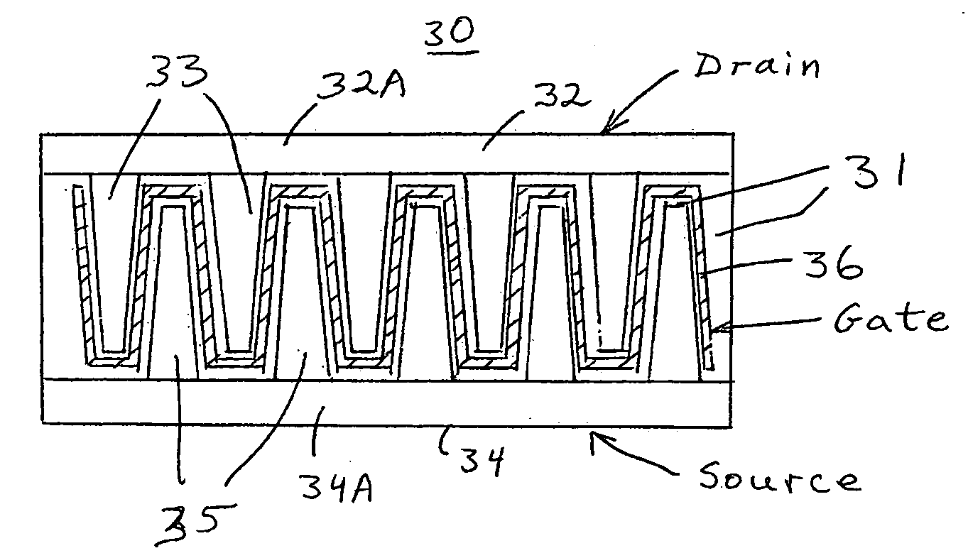
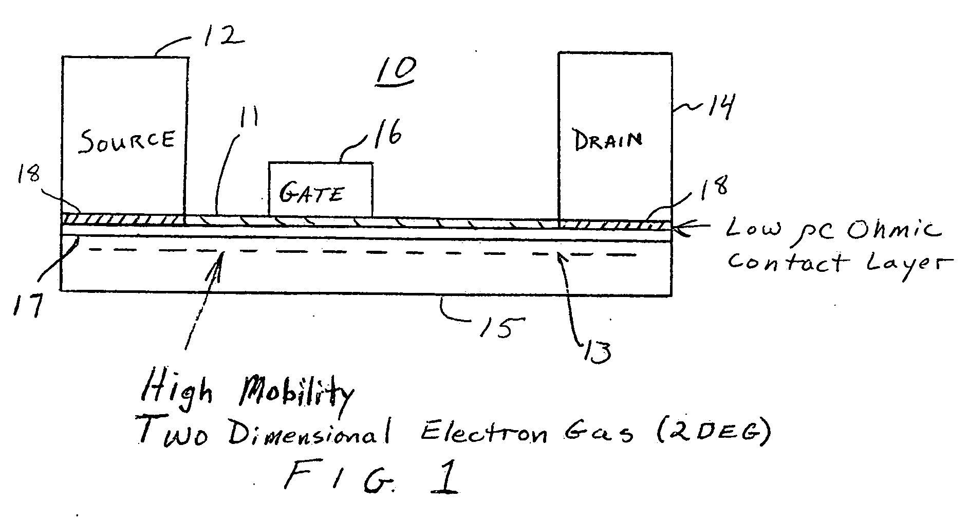
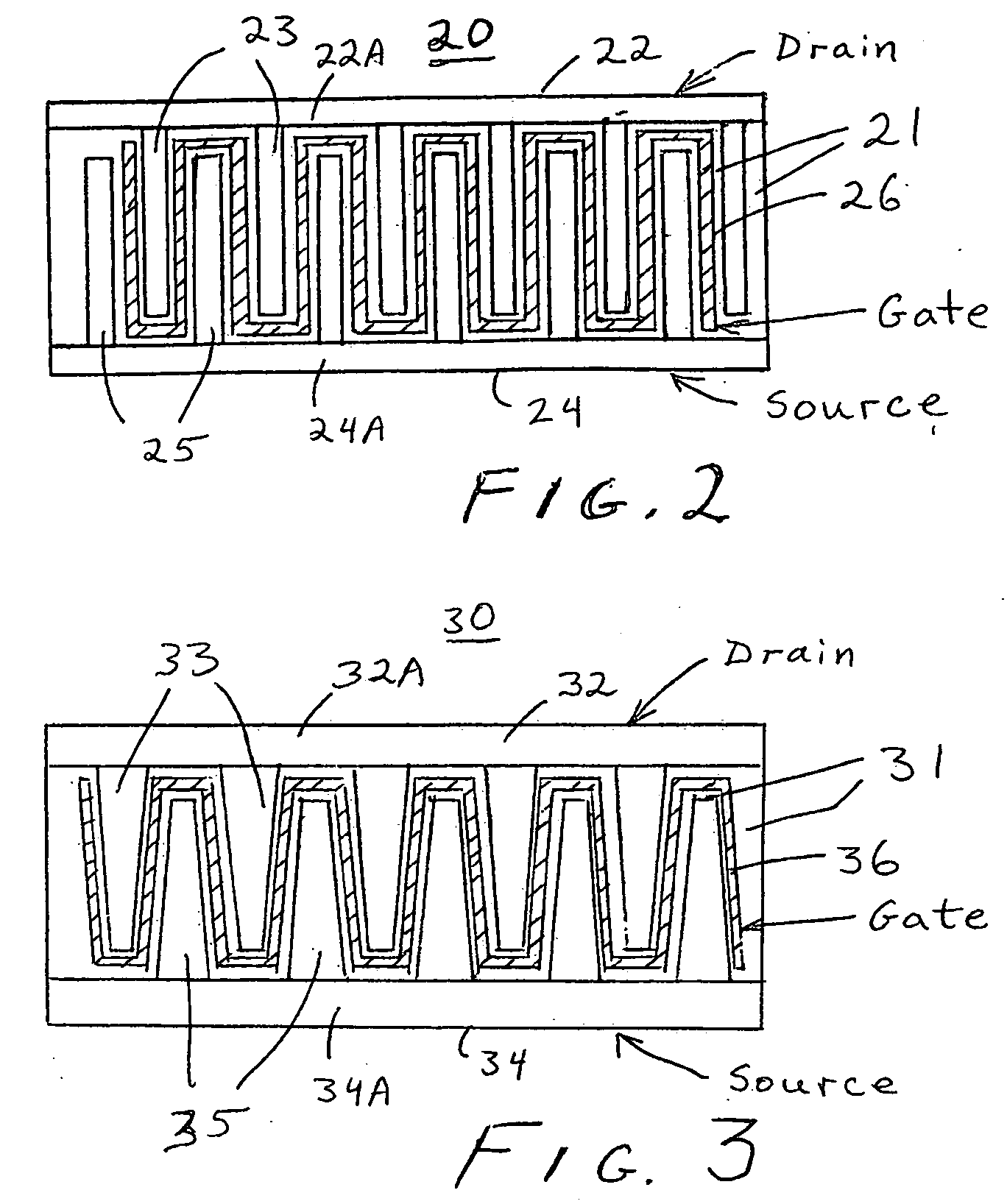
[0027] In the construction of GaN material devices, a number of factors come into play to impact the functionality and capability of the devices. A large lattice mismatch in III-nitride materials and the strong piezoelectric and polarization effects in these materials significantly impact the electrical properties of III-nitride heterojunction devices. Nearly all reported GaN-based HEMTs to date use strained GaN—AlGaN junctions with alloy compositions that are designed to maximize the strain in the AlGaN layer but avoid producing long term instabilities in the AlGaN layer or device. Various devices and systems for building heterojunction devices have been proposed to control the lattice mismatch and the strain of the GaN—AlGaN junctions. These devices are particularly designed to take advantage of piezoelectric and spontaneous polarization effects and to minimize long term instabilities.

[0028] GaN / AlGaN HEMT devices typically have three terminals including a gate, a drain and a sou...


PUM


Abstract

A III-nitride power device for controlling high currents as an interdigitated electrode pattern for increasing device rating while decreasing device dimensions. Fingers of the interdigitated electrode pattern have tips with smaller dimensions than the remainder of the fingers. The tapered finger design balances current flow in the electrode fingers to reduce device resistance while permitting a more compact construction.

Description

CROSS-REFERENCE TO RELATED APPLICATION [0001] The present application is based on and claims benefit of U.S. Provisional Application No. 60 / 527,576, filed Dec. 5, 2003, entitled AlGaN / GaN Field Effect Transistor Design with Optimal Finger Design, to which a claim of priority is hereby made, and the entire contents of which are hereby incorporated herein by reference.BACKGROUND OF THE INVENTION [0002] 1. Field of the Invention [0003] The present invention relates generally to a class of field effect transistors based on III-nitride materials, and relates more particularly to a field effect transistor layout geometry for carrying high current. [0004] 2. Description of Related Art [0005] Column III-nitride alloy used in semiconductors, including AlN, GaN and InN may be used to produced devices that exhibit large dielectric breakdown fields, and are capable of high power, high frequency switching. A typical application for III-nitride semiconductors is in the construction of emitters fo...

Claims


Application Information

Patent Timeline
Patent Type & Authority Applications(United States)
IPC IPC(8): H01L29/06H01L29/20H01L29/423H01L29/778
CPCH01L29/0692H01L29/2003H01L29/41758H01L29/7787H01L29/42316
Inventor BEACH, ROBERTBRIDGER, PAUL
Owner INFINEON TECH AMERICAS CORP
Why Eureka
Try Eureka