
Semiconductor device and manufacturing process therefor as well as plating solution

a technology of semiconductor devices and manufacturing processes, applied in semiconductor devices, semiconductor/solid-state device details, electrical devices, etc., can solve the problems of reducing the yield of semiconductor devices, less information about the physical properties of such alloy films and their effects on device performance, and increasing the impact of mass transfer through such a grain boundary, so as to improve the reliability of devices and improve the effect of stress migration resistan

Inactive Publication Date: 2005-06-30
RENESAS ELECTRONICS CORP
View PDF8 Cites 17 Cited by
  • Summary
  • Abstract
  • Description
  • Claims
  • Application Information

AI Technical Summary

Benefits of technology

[0015] In view of these problems, an objective of this invention is to improve stress migration resistance in a semiconductor device comprising a metal region, and thus to improve reliability of the device.
[0019] The metal region in the above semiconductor device a larger amount of silver than that in a conventional interconnection structure made of a copper-silver alloy, and thus can effectively prevent stress migration when being exposed to a heat history during, for example, a process for manufacturing a semiconductor.
[0021] When a semiconductor device is exposed to a heat history, a temperature-stress curve for a metal region generally exhibits different patterns in a warming and a cooling processes. An indicator for the difference is defined as a “maximum hysteresis error”. A maximum hysteresis error is the maximum separation width between the curves showing the warming and the cooling processes. For example, in FIG. 8, the maximum width between a warming process a and a cooling process b is a maximum hysteresis error. In the semiconductor device, an irreversible loss is reduced when being exposed to a heat history during a process for manufacturing a semiconductor, and thus stress migration is effectively prevented.
[0022] This invention further provides a semiconductor device comprising a metal region on a semiconductor substrate wherein a recrystallization temperature of a component metal in the metal region is 200° C. or higher. A recrystallization temperature is a temperature at which transformation of crystal grains or grain growth occurs due to atomic diffusion. Since recrystallization may result in a void or distortion in a metal region, a higher recrystallization temperature is an important condition for providing a reliable metal region. The above semiconductor device has a recrystallization temperature higher than 200° C., so that irreversible loss can be minimized when being exposed to a heat history and thus stress migration can be effectively prevented. A recrystallization temperature can be determined by, for example, measuring a hysteresis curve. FIG. 9 shows a method for determining a recrystallization temperature. An inflection point during a warming process, i. e., an intersection between a linear line and a horizontal line after the initiation of temperature-rising corresponds to a recrystallization temperature. In this figure, a recrystallization temperature is 220° C.
[0025] According to this process for manufacturing a semiconductor device, contacting the surface of the metal region with a silver-containing liquid results in precipitation of silver and then heating allows silver to diffuse in the metal region. As a result, a silver-containing metal region may be suitably formed. According to this invention, a metal region made of a copper-silver alloy may be consistently formed by a convenient process. Since a plating solution itself does not have to contain silver, the plating solution may be selected more freely.
[0032] When a metal region in this invention is made of a copper-silver alloy, other components may be further added. For example, components such as Zr, In, Al, Ti and Sn may be added up to 1 wt % to the total amount of the metals. Zr and / or In may be added to improve adhesiveness between the metal region and an insulating film and / or between the metal region and a barrier metal film. Al, Ti and Sn may diffuse in the surface of the reactive copper-silver alloy film to be bound to the material atoms constituting the interlayer insulating film, resulting in improved adhesiveness.

Problems solved by technology

In a narrower interconnection, a copper grain size is smaller and thus the problem of migration due to mass transfer via such a grain boundary becomes more significant.
There have been developed no methods for consistently forming an alloy containing silver and copper with a silver content higher than the above limit and thus there have been little information about the physical properties of such an alloy film and its effects on device performance when applied in a semiconductor device.
A void thus formed may cause connection defect between a connecting plug and an interconnection, a reduced yield of a semiconductor device and instability in a semiconductor device after a long period use.

Method used


Image

  • Semiconductor device and manufacturing process therefor as well as plating solution
  • Semiconductor device and manufacturing process therefor as well as plating solution
  • Semiconductor device and manufacturing process therefor as well as plating solution

Examples


example 1

[0124] Metal interconnections in FIG. 17 were formed by a damascene process. All of these interconnections had dimensions of 0.1 to 0.5 μm (width)×0.3 μm (thickness)×49 mm (length), and silver contents in an interconnection metal were 0, 1.5 and 2.0 wt %. The interconnection was formed by plating using a chloride-ion free plating solution. For the interconnections thus formed, an interconnection resistance was determined and the results shown in FIG. 17 were obtained. This figure shows that resistance increase was inhibited in the interconnection structures in which a silver content to the total amount of the component metals in an interconnection is 1.5 wt % or more. In a copper-silver alloy, a relationship between atom % and wt % is such that, for example, a silver content of 0.9 atom % corresponds to 1.5 wt %.

example 2

[0125] In this example, a two-layer interconnection structure shown in FIG. 10 was formed to test an yield. This two-layer interconnection structure is called a via chain, in which first interconnections 22a are formed in parallel and second interconnections 22b perpendicular to them are formed. The width of the interconnections should be wide such as 5 micron to test the stress-migration reliability effectively. These interconnections are connected to each other via 20,000 connecting plugs 28. In this figure, a semiconductor substrate and an interlayer insulating film are omitted. A given voltage can be applied to the ends of the via chain to measure an electric resistance through 10,000 first interconnections 22a, 10,000 second interconnections 22b and 20,000 connecting plugs 28. The resistance is called a chain resistance, which is an effective indicator to determine the quality of the via connection. While the interconnection structure is placed under given thermal environment, ...

example 3

[0129] For evaluating material properties for the samples in Examples 1 and 2, hysteresis properties and recrystallization temperatures were determined.

[0130] Samples were prepared as follows. On a silicon substrate was deposited a silicon oxide film to 500 nm by plasma CVD, on which was then deposited a Ta film to 50 nm. Then, on the upper surface was deposited a copper plating seed film to 100 to 200 nm by sputtering, on which was then deposited a copper or copper-silver alloy film to 600 to 700 nm using a given plating solution. A composition of the copper or copper-silver alloy film was described in Table 2, in which plating solution 1 contains chloride ions while plating solution 2 does not.

[0131] The samples thus prepared were exposed to thermal cycles of 25° C. to 400° C. In this heat history, a warming rate was 10° C. / min in the warming process while a cooling rate was about 10° C. / min in the cooling cycle. The thermal cycle was repeated twice and hysteresis properties wer...


PUM

PropertyMeasurementUnit
Percent by massaaaaaaaaaa
Dissociation constantaaaaaaaaaa
Concentrationaaaaaaaaaa

Abstract

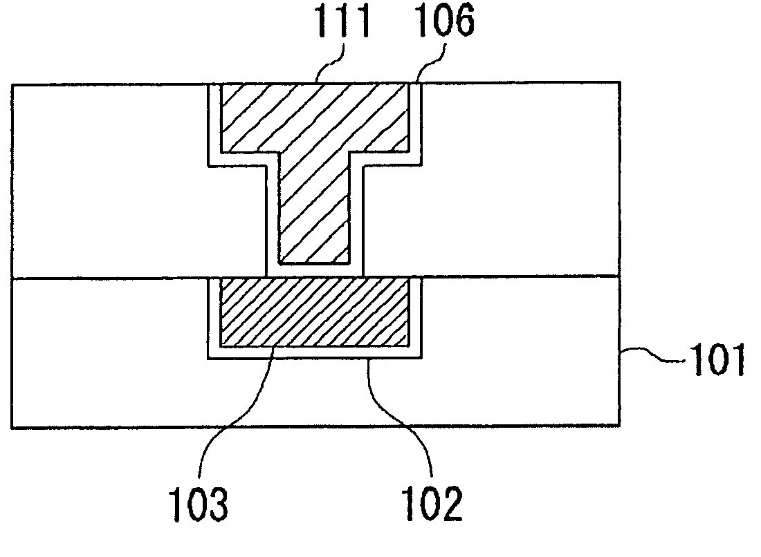
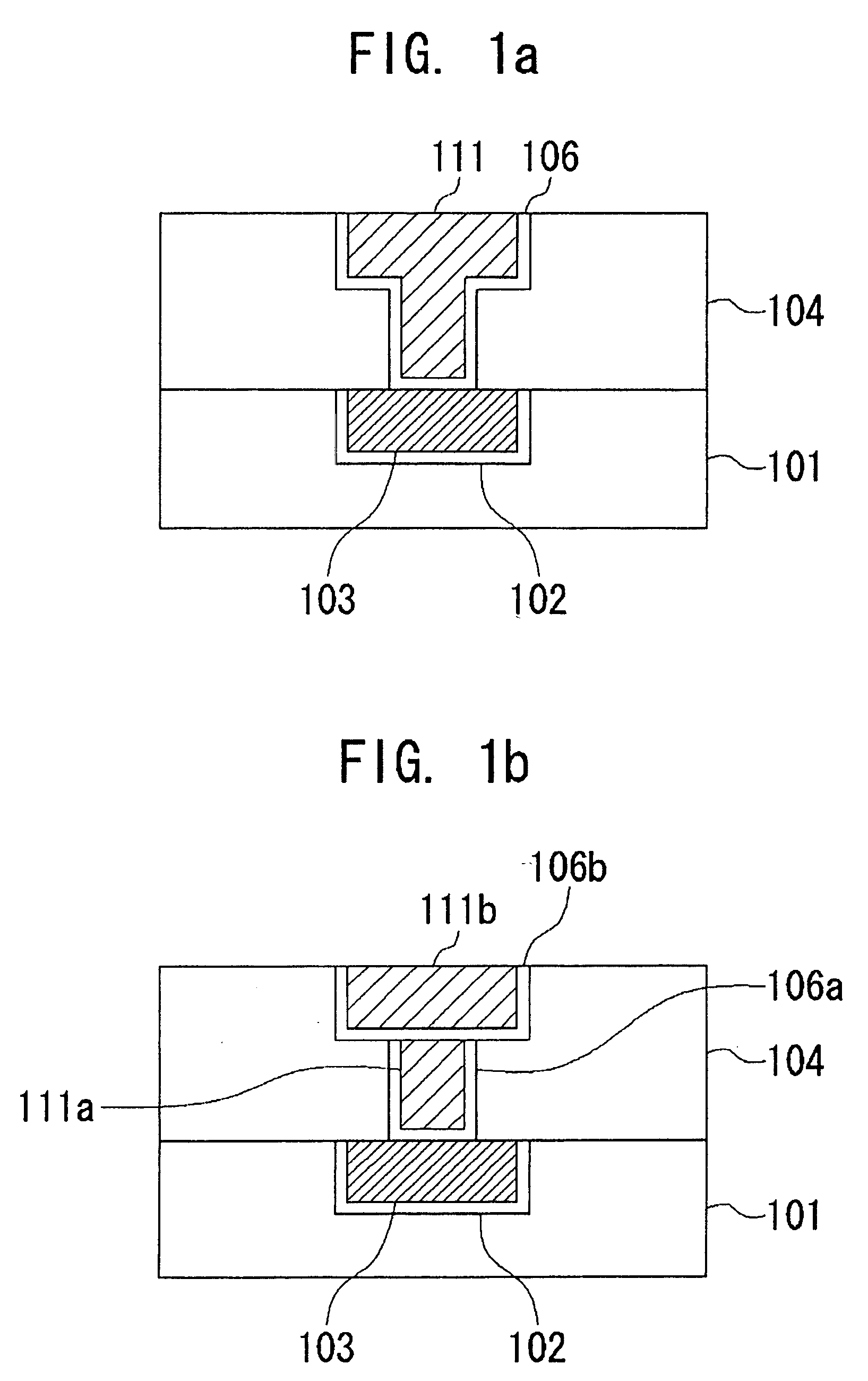
A semiconductor device of improved stress-migration resistance and reliability includes an insulating film having formed therein a lower interconnection consisting of a barrier metal film and a copper-silver alloy film, on which is then formed an interlayer insulating film. In the interlayer insulating film is formed an upper interconnection consisting of a barrier metal film and a copper-silver alloy film. The lower and the upper interconnections are made of a copper-silver alloy which contains silver in an amount more than a solid solution limit of silver to copper.

Description

[0001] This application is based on Japanese patent application NO. 2002-127702, the content of which is incorporated hereinto by reference. BACKGROUND OF THE INVENTION [0002] 1. Field of the Invention [0003] This invention relates to a semiconductor device comprising a silver-containing metal region and a process for manufacturing the device. [0004] 2. Description of the Prior Art [0005] Recent increasing integration of a semiconductor device has required the use of copper as a material for an interconnection or plug. Copper has advantageous properties of a lower resistance and higher electromigration resistance compared with aluminum which has been conventionally used. [0006] However, as a device has become more compact, electromigration has been significant in such an interconnection using copper. A copper film as a copper interconnection is usually formed by plating, which gives the copper film as an aggregate of a number of polycrystalline copper grains. When a voltage is appli...

Claims


Application Information

Patent Timeline
IPC IPC(8): C25D7/12H01L21/288H01L21/768H01L23/522H01L23/532
CPCH01L21/288H01L21/2885H01L21/76807H01L21/76843H01L21/76877H01L23/5226H01L2924/0002H01L23/53233H01L23/53238H01L2924/00
Inventor UENO, KAZUYOSHI
Owner RENESAS ELECTRONICS CORP
Learn More