Technique for perfecting the active regions of wide bandgap semiconductor nitride devices

Inactive Publication Date: 2005-07-28
THE UNITED STATES OF AMERICA AS REPRESENTED BY THE SECRETARY OF THE NAVY
View PDF16 Cites 83 Cited by
  • Summary
  • Abstract
  • Description
  • Claims
  • Application Information

AI Technical Summary

Benefits of technology

[0012] Another object of this invention is a way to enhance thickness of active material without causing cracking therein.
[0013] These and other objects of this invention can be attained by depositing a mask material on a substrate; patterning the mask material to form openings in the mask mate

Problems solved by technology
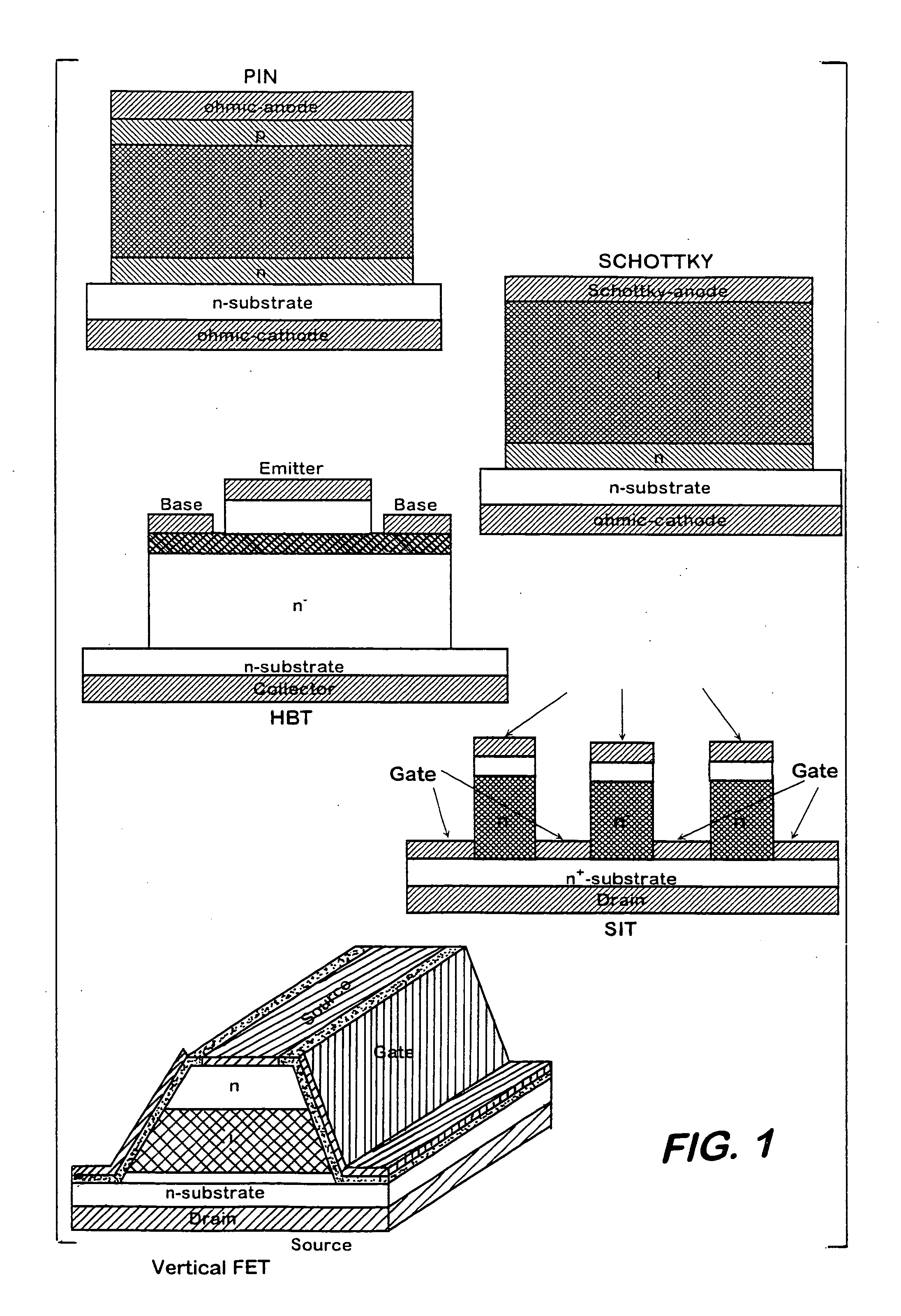
Despite this considerable promise, a fundamental hurdle has limited progress in realizing some of these device technologies.
That hurdle is a lack of native substrate that would permit homoepitaxy.
Further, these and related defects result in compensated films that make it difficult to controllably dope the material at low levels consistent with blocki

Method used


Image

  • Technique for perfecting the active regions of wide bandgap semiconductor nitride devices
  • Technique for perfecting the active regions of wide bandgap semiconductor nitride devices
  • Technique for perfecting the active regions of wide bandgap semiconductor nitride devices

Examples


Example

EXAMPLE I

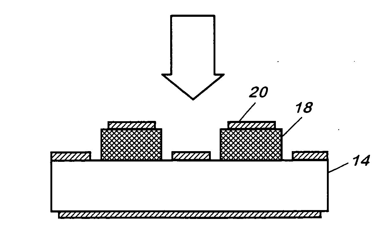
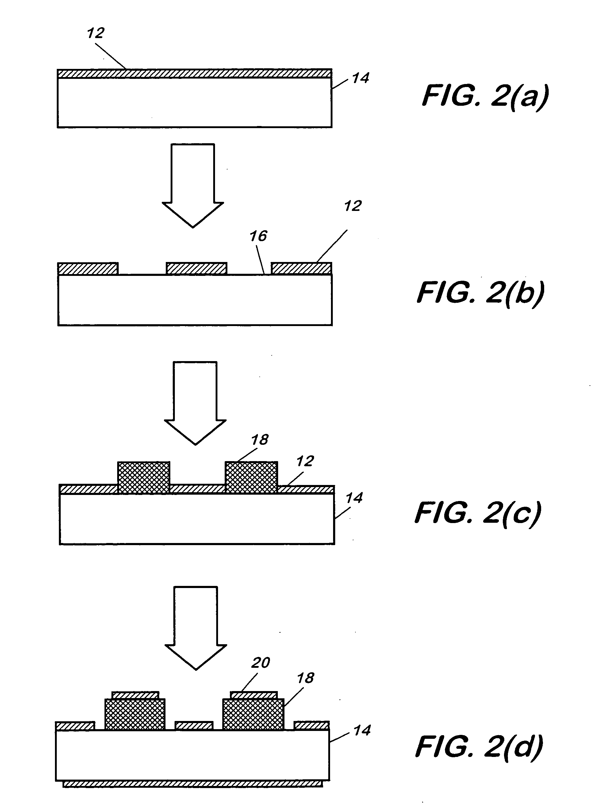
[0037] This example illustrates confined growth of an electronic device fabricated by the use of the lift-off procedure for removing resist and oxide mask materials in the growth areas.

[0038] Pursuant to the objectives herein, the substrate used was a sapphire disk 5 cm in diameter and 330-micron thick coated with a 3-micron thick layer of gallium nitride starting layer that was cleaned before any processing using a standard solvent series ultrasonic cleaning. The polymethylmethacrylate resist of several hundred angstroms thickness was spun on the substrate, and processed using standard lithographic techniques that left the resist only in areas that were ultimately to be grown upon. A blanket mask coating 1000 angstroms thick of the dielectric thin film silicon dioxide was uniformly deposited on the resist using reactive sputter deposition. The principal purpose of the mask material herein was to provide confined growth of the gallium nitride active material. The sample w...


PUM


Abstract

This invention pertains to e lectronic/optoelectronic devices with reduced extended defects and to a method for making it. The method includes the steps of depositing a dielectric thin film mask material on a semiconductor substrate surface; patterning the mask material to form openings therein extending to the substrate surface; growing active material in the openings; removing the mask material to form the device with reduced extended defect density; and depositing electrical contacts on the device.

Description

BACKGROUND OF THE INVENTION [0001] 1. Field of the Invention [0002] This invention pertains to wide bandgap electronic devices, such as high frequency and high power devices; optoelectronic devices, such as visible light emitters to ultraviolet lasers and detectors; and a method for making such devices. [0003] 2. Description of Related Art [0004] Wide bandgap semiconductor nitrides have demonstrated and continue to hold significant promise in a wide range of device technologies. This family of semiconductors has a tunable direct bandgap that ranges from 8 eV up to 6.2 eV, covering the IR, visible, and UV portions of the electomagnetic spectrum making them well suited to optoelectronic applications from visible light emitters to UV lasers and detectors. It is this application area that has received the most commercial attention to date, resulting in billion dollar LED industries. Perhaps the largest promise from wide bandgap semiconductor nitrides is yet to be fulfilled, that being i...

Claims


Application Information

Patent Timeline
IPC IPC(8): C30B25/04C30B29/40H01L21/20H01L21/205H01L29/20
CPCC30B25/04C30B29/40H01L29/2003H01L21/0237H01L21/02639H01L21/0242H01L21/0254H01L21/0262H01L21/02378
Inventor PECKERAR, MARTINHENRY, RICHARDKOLESKE, DANIELWICKENDEN, ALMAEDDY, CHARLES R. JR.HOLM, RONALDTWIGG, MARK E.
Owner THE UNITED STATES OF AMERICA AS REPRESENTED BY THE SECRETARY OF THE NAVY
Why Eureka
Try Eureka