Zirconium oxide and hafnium oxide etching using halogen containing chemicals

a technology of hafnium oxide and zirconium oxide, which is applied in the direction of semiconductor devices, basic electric elements, electrical equipment, etc., can solve the problems of inability to avoid the problem of tunneling current, inability to remove the over isolation region easily, and conventional plasma etching methods do not provide a high selective level for zrosub>2 /sub>or hfo

Active Publication Date: 2005-07-28
TAIWAN SEMICON MFG CO LTD
View PDF6 Cites 233 Cited by
  • Summary
  • Abstract
  • Description
  • Claims
  • Application Information

AI Technical Summary

Benefits of technology

[0009] One objective of the present invention is to provide an efficient means of removing a high k dielectric layer comprised of one or more of ZrO2, HfO2,Ta2O5, TiO2, Al2O3, Y2O3 and La2O5 or a nitride, silicate, or oxynitride of Zr, Hf, Ta, Ti, Al, Y, and La from a substrate without forming a residue.

Problems solved by technology

Below that thickness, a tunneling current problem cannot be avoided.
One problem associated with high k dielectric layers is that they are not easily removed from over isolation regions or over areas of the substrate that will become source / drain (S / D) regions.
Conventional plasma etch methods do not provide a high enough selectively for ZrO2 or HfO2, for example, relative to SiO2 above isolation regions or relative to silicon above S / D regions in the substrate.
Furthermore, ZrO2 and HfO2 have an etch rate that is too slow to be useful in the buffered HF treatment that is effective in removing silicon oxide.
Moreover, the method should not form high k dielectric etch residues which are difficult to remove.

Method used


Image

  • Zirconium oxide and hafnium oxide etching using halogen containing chemicals
  • Zirconium oxide and hafnium oxide etching using halogen containing chemicals
  • Zirconium oxide and hafnium oxide etching using halogen containing chemicals

Examples


first embodiment

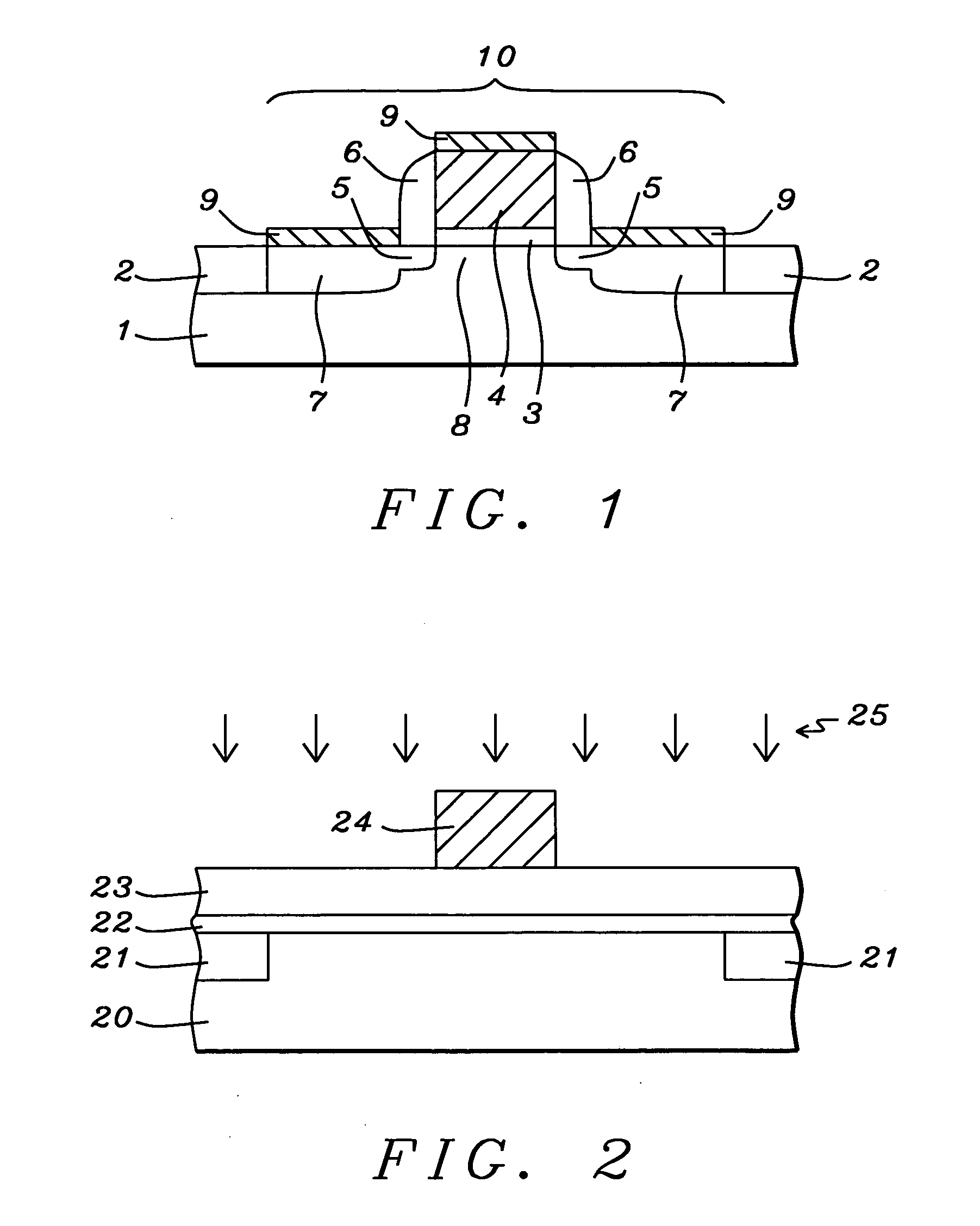
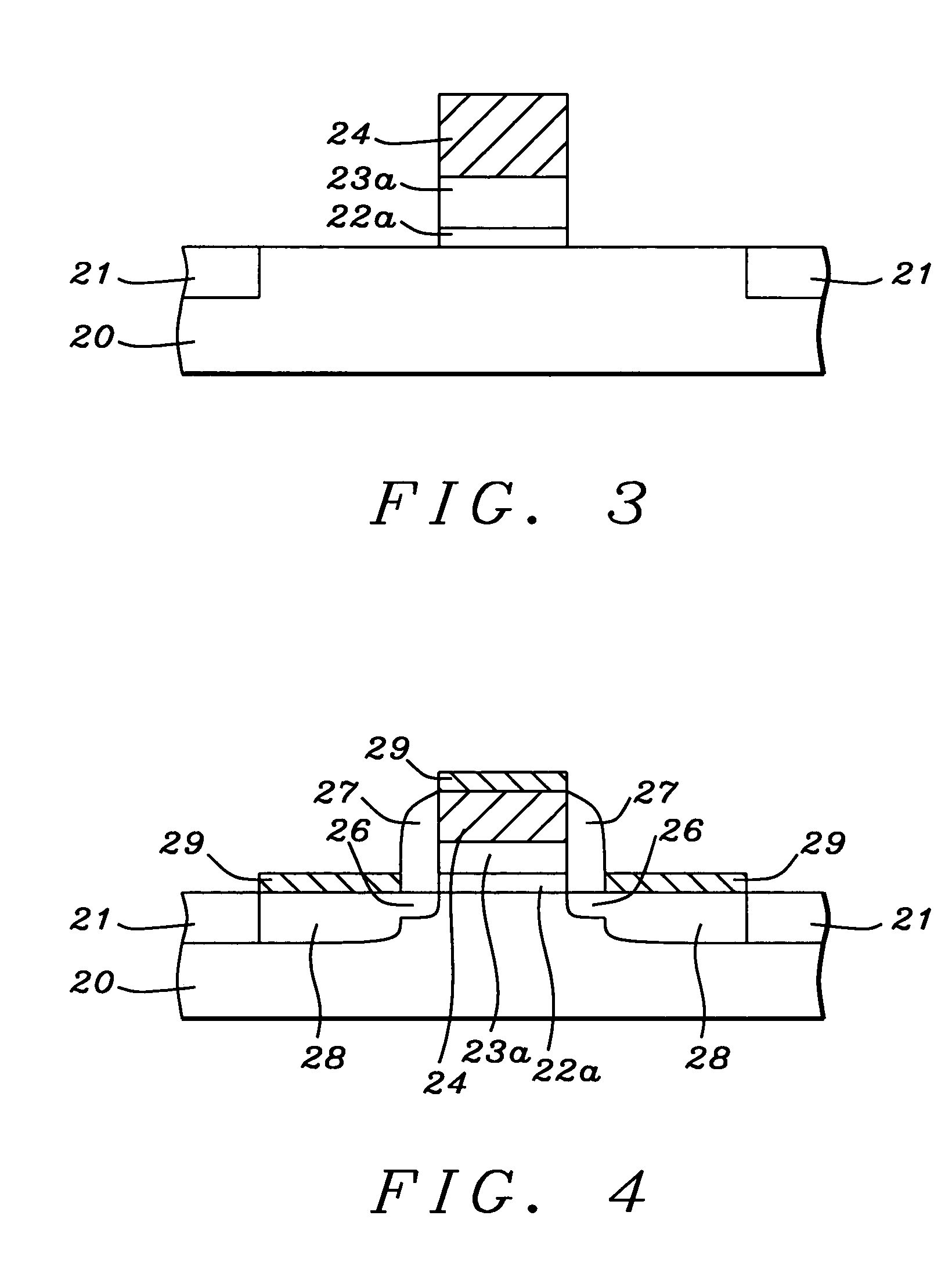
[0026] The first embodiment is set forth in FIGS. 2-4. Referring to FIG. 2, a substrate 20 is provided which may include active and passive devices. Substrate 20 is typically silicon and has an n-well or a p-well (not shown) depending on the type of transistor that will subsequently be formed. Isolation regions 21 are formed in the substrate 20 by conventional methods and are generally comprised of silicon oxide or a low k dielectric material such as carbon doped SiO2 or fluorine doped SiO2. In the exemplary embodiment, an isolation region 21 is shown as a shallow trench isolation (STI) region but optionally may be a field oxide (FOX) structure or a mesa isolation region. In one embodiment, a thin interfacial layer 22 with a thickness between about 1 and 30 Angstroms is deposited on substrate 20 and is comprised of a material such as silicon oxide, silicon nitride or silicon oxynitride. The interfacial layer 22 is preferably formed by a rapid thermal process (RTP) although a low pre...

second embodiment

[0037] the invention involves the use of a high k dielectric layer as a hard mask during a pattern transfer process. The second embodiment is illustrated in FIGS. 5-7. Referring to FIG. 5, a substrate 30 is provided which may include active and passive devices. Substrate 30 may be comprised of silicon, SiGe, silicon-on-insulator (SOI), or other semiconductor materials used in the art. Optionally, the substrate 30 may be a dielectric layer or a semiconductive material. In another embodiment, a thin interfacial layer (not shown) such as silicon nitride, silicon oxide, or silicon oxynitride is formed on the substrate 30 by a CVD or PECVD process. An interfacial layer is employed to provide a smoother interface between the substrate 30 and an overlying high k dielectric layer 31.

[0038] A high k dielectric layer 31 which is preferably a zirconium or hafnium oxide, silicate, nitride or oxynitride is deposited by an ALD, CVD, or MOCVD technique on the substrate 30. However, those skilled i...

third embodiment

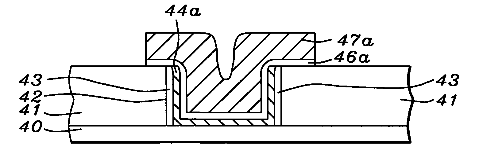
[0047] A third embodiment is illustrated in FIGS. 8-11 in which a capacitor is fabricated that includes a first conducting layer formed within an opening in an ILD layer, a high k dielectric layer on the first conducting layer and ILD layer, and a second conducting layer on the high k dielectric layer. A key feature is selectively removing portions of the high k dielectric layer on the ILD layer. The high k dielectric etch process of this embodiment may be used for various types of capacitors including but not limited to metal-insulator-metal (MIM), metal-insulator-polysilicon (MIP), polysilicon-insulator-polysilicon (PIP), and metal-insulator-silicon (MIS). Furthermore, the present invention is not restricted to the capacitor structure depicted in FIGS. 8-11.

[0048] Referring to FIG. 8, a substrate 40 is shown that may be a dielectric layer such as silicon nitride, for example, with a metal plug (not shown) formed within. An interlevel dielectric (ILD) layer 41 is deposited by a CVD...


PUM


Abstract

A method is described for selectively etching a high k dielectric layer that is preferably a hafnium or zirconium oxide, silicate, nitride, or oxynitride with a selectivity of greater than 2:1 relative to silicon oxide, polysilicon, or silicon. The plasma etch chemistry is comprised of one or more halogen containing gases such as CF4, CHF3, CH2F2, CH3F, C4F8, C4F6, C5F6, BCl3, Br2, HF, HCl, HBr, HI, and NF3 and leaves no etch residues. An inert gas or an inert gas and oxidant gas may be added to the halogen containing gas. In one embodiment, a high k gate dielectric layer is removed on portions of an active area in a MOS transistor. Alternatively, the high k dielectric layer is used in a capacitor between two conducting layers and is selectively removed from portions of an ILD layer.

Description

FIELD OF THE INVENTION [0001] The invention relates to a method of fabricating semiconductor devices. More particularly, the present invention is a method of selectively removing a high k dielectric layer from a substrate. BACKGROUND OF THE INVENTION [0002] As the gate length in transistors shrinks in order to keep pace with demands for improved performance, the thickness of the gate electrode and the gate dielectric layer are following a trend toward thinner films. Shrinking device dimensions force a thinner dielectric layer in order to maintain an adequate capacitance between the gate electrode and the channel region. Traditional gate dielectric layers consisting of silicon oxide with a dielectric constant of about 4 have reached a minimum limit for thickness at about 1 nm. Below that thickness, a tunneling current problem cannot be avoided. [0003] A typical transistor is shown in FIG. 1 and is comprised of a substrate 1 with isolation regions 2 that separate an active region 10 f...

Claims


Application Information

Patent Timeline
Patent Type & Authority Applications(United States)
IPC IPC(8): H01L21/20H01L21/28H01L21/311H01L21/316H01L21/3205H01L21/336H01L21/8242H01L29/51
CPCH01L21/28194H01L21/31122H01L21/31641H01L29/66583H01L29/513H01L29/517H01L29/665H01L21/31645H01L21/3065
Inventor PERNG, BAW-CHINGCHIU, YUAN-HUNGSUNG, MEI-HUIHSU, PENG-FU
Owner TAIWAN SEMICON MFG CO LTD
Why Eureka
Try Eureka