Stress-tuned, single-layer silicon nitride film

a silicon nitride film, single-layer technology, applied in the direction of chemical vapor deposition coating, coating, plasma technique, etc., can solve the problem of more difficult to deposit a thin film, achieve high voltage to wattage (v/w), enhance stress tunability, and control the amount of wattag

Inactive Publication Date: 2005-08-04
APPLIED MATERIALS INC
View PDF20 Cites 89 Cited by
  • Summary
  • Abstract
  • Description
  • Claims
  • Application Information

AI Technical Summary

Benefits of technology

[0022] In both instances, for the 200-mm diameter wafer and the 300-mm diameter wafer, the power from a low frequency generator assembly is mixed with the power from a high frequence generator assembly prior to application of the plasma generation power to the process chamber. The benefit of using a 100 W low frequency generator is that a high voltage to wattage (V/W) resolution is achieved. A 1000 W low frequency generator would typically provide a V/W ratio of about 0.01 V/W, where the 100 W generator would typically provide a ratio of about 0.10 V/W, for the apparatus referenced above. This permits a careful control over the amount of wattage applied to the plasma via adjustment of the low frequency input, since the output from the low frequency generator is much less susceptible to noise (due to a higher voltage) than the output from the hi

Problems solved by technology

In the past, silicon nitride individual layers typically had a thickness in the range of about 1400 Å, with an overall film thickness in the range of about 10,000 Å. While it is possible to deposit the thicker films of at least 1400 Å, for example, whle controlling the stress

Method used


Image

  • Stress-tuned, single-layer silicon nitride film
  • Stress-tuned, single-layer silicon nitride film
  • Stress-tuned, single-layer silicon nitride film

Examples


Embodiment Construction

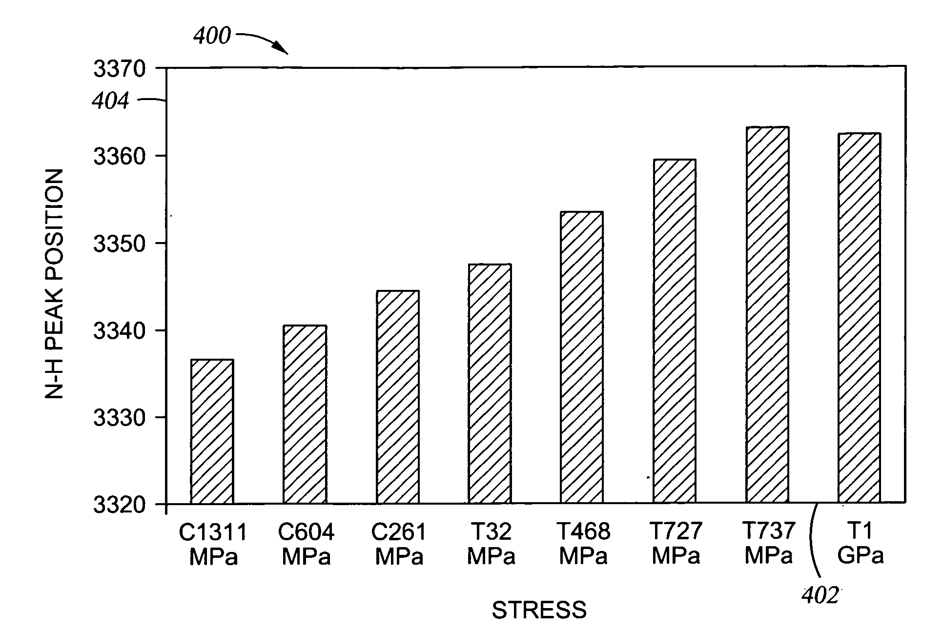
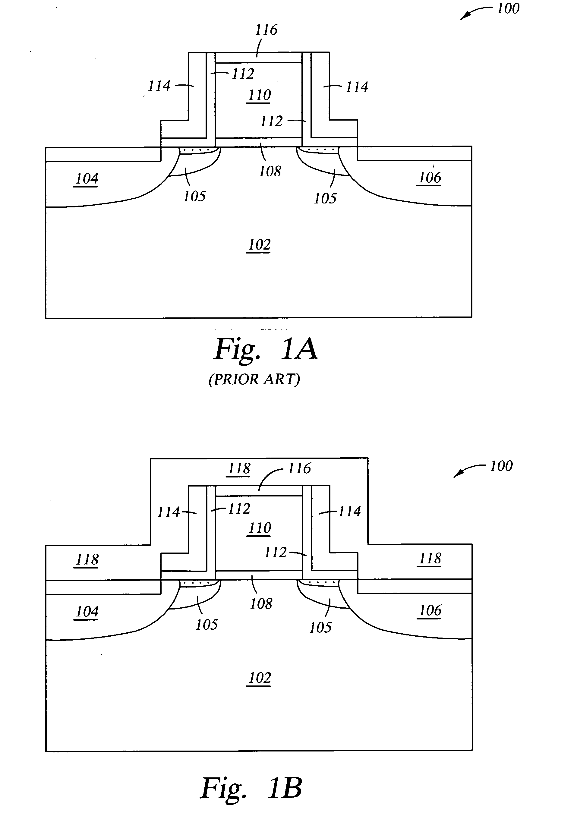
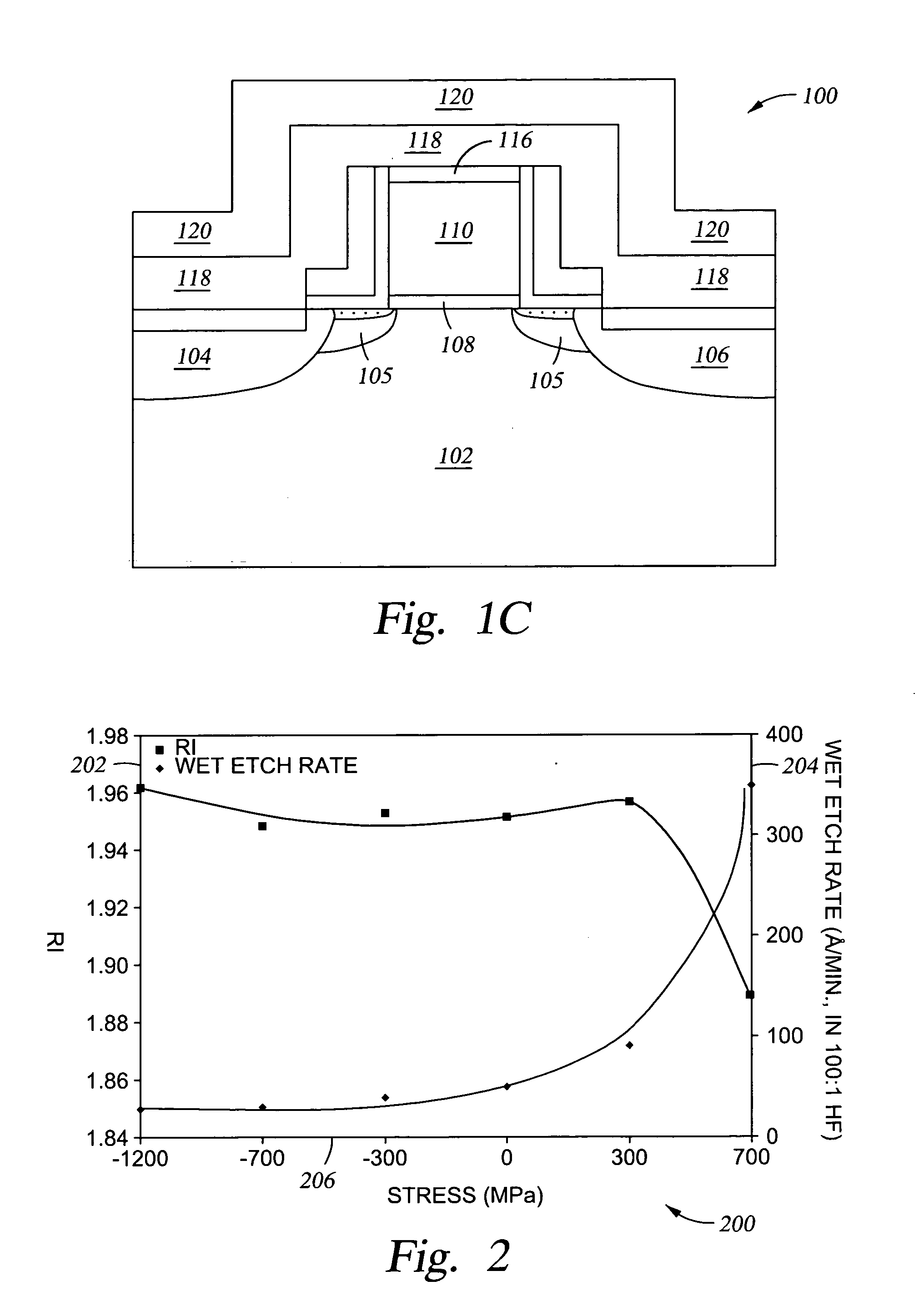
[0065] Disclosed herein is a method of tuning the stress of a single-layer, homogeneous silicon nitride film over a broad range previously unattainable. The exemplary processing conditions for performing various embodiments of the method of the invention set forth below are not intended to limit the scope of the inventive concept provided herein.

[0066] As a preface to the detailed description, it should be noted that, as used in this specification and the appended claims, the singular forms “a”, “an”, and “the” include plural referents, unless the context clearly dictates otherwise.

[0067] I. An Apparatus for Practicing the Invention

[0068]FIG. 3A is a top view schematic of a multi-chamber processing system of the kind which may be used to carry out the method described herein, a PRODUCER®, available from Applied Materials, Inc. (Santa Clara, Calif.). The PRODUCER®processing platform is used to support a fully automated substrate processing system employing a single-substrate, mult...


PUM

PropertyMeasurementUnit
Temperatureaaaaaaaaaa

Abstract

We have discovered that is possible to tune the stress of a single-layer silicon nitride film by manipulating certain film deposition parameters. These parameters include: use of multiple (typically dual) power input sources operating within different frequency ranges; the deposition temperature; the process chamber pressure; and the composition of the deposition source gas. In particular, we have found that it is possible to produce a single-layer, thin (300 Å to 1000 Å thickness) silicon nitride film having a stress tuned to be within the range of about −1.4 GPa (compressive) to about +1.5 GPa (tensile) by depositing the film by PECVD, in a single deposition step, at a substrate temperature within the range of about 375° C. to about 525 ° C., and over a process chamber pressure ranging from about 2 Torr to about 15 Torr.

Description

FIELD OF THE INVENTION [0001] The present invention pertains to a stress-tuned, single-layer silicon nitride film and to a method of depositing the silicon nitride film using plasma-enhanced chemical vapor deposition (PECVD). BRIEF DESCRIPTION OF THE BACKGROUND ART [0002] An important element of transistor scaling and improved drive current performance for semiconductor devices is the mobility of the carriers in the channels of the device. One approach for enhancing the mobility is the induction of strain in a silicon lattice, to modify the structure of silicon and thus enhance the electron mobility or hole mobility. [0003] U.S. Pat. No. 5,155,571, to Wang et al., issued Oct. 13, 1992, describes the increase in carrier mobility for both electrons and holes in complementary field effect transistor structures, such as CMOS and CMOD. The increased carrier mobility is obtained by using strained GexSi1-x / Si layers for the carrier conduction channels. There is said to be an advantage in i...

Claims


Application Information

Patent Timeline
IPC IPC(8): C23C16/34H01L21/314H01L21/318
CPCC23C16/345H01J37/32165H01L29/7843H01L29/7842H01L21/3185H01L21/02274H01L21/0217
Inventor JUNG, KEEBUMTANG, SUM-YEE BETTYSEAMONS, MARTIN JAYARGHAVANI, REZAJUCO, ELLER Y.
Owner APPLIED MATERIALS INC
Why Eureka
Try Eureka