Semiconductor element and method for producing the same

a semiconductor and element technology, applied in the direction of semiconductor lasers, semiconductor laser structural details, manufacturing tools, etc., can solve the problems of troublesome work, difficult processing, and difficulty in division compared with semiconductor elements made of other materials, and achieve the effect of improving reflecting efficiency and solving efficiently

Inactive Publication Date: 2005-08-25
TOYODA GOSEI CO LTD
View PDF5 Cites 105 Cited by
  • Summary
  • Abstract
  • Description
  • Claims
  • Application Information

AI Technical Summary

Benefits of technology

[0026] An object of the invention is to provide individual semiconductor elements obtained by dividing a substrate easily with a good yield and low cost and another object of the invention is to remove melt of a substrate from outer circumferences of elements after division as much as possible.

Problems solved by technology

Substrates made of these materials differ from substrates using silicon and gallium arsenide in that they are not easy to process.
Accordingly, when a wafer obtained by lamination of Group III nitride compound semiconductors on a substrate made of one of these materials is divided into individual elements, the division is attended with difficulty compared with semiconductor elements made of other materials.
This is very troublesome work requiring trial and error.
The proposals, however, have been not put into practical use yet in production of Group III nitride compound semiconductor elements.
When separation grooves are formed by laser beam irradiation, substrate and semiconductor materials are melted and vaporized so that element surfaces are contaminated with reaction products.
As a result, light-extracting efficiency of each of the light-emitting elements is reduced.
In addition, the molten semiconductor may form an undesirable short circuit to spoil element characteristic remarkably or a dividing method for producing a very small number of acceptable products may be provided according to circumstances.
Because the molten layer is not translucent so that light emitted from a light-emitting layer is absorbed to the molten layer, the molten layer is a a main cause of reduction in external quantum efficiency of the LED.
As a result, the upper surface of the semiconductor layer is contaminated.
Such a contaminant (deposit) is also a main cause of reduction in external quantum efficiency of the semiconductor light-emitting element.
Generally, before dicing, the metal layer is removed from the region indicated by the distance Δ. A scribing cutter or a dicing cutter is generally expensive because it is often made of a large number of diamond grains (pieces) gathered together.
If the dicing process is executed without removal of the metal layer, the expensive cutter is clogged soon so that the cutter cannot be used any more.
This is because there is a limit to shape accuracy of the cutter, positioning accuracy of the cutter, processing accuracy in removal of the metal layer, etc.
Furthermore, when the separation groove S is made deep, the width of the separation groove S is apt to increase inevitably.
Although this width is surely smaller than the width (30 μm or larger) of the separation groove S formed by the cutter, the problem of deposit (contaminant) occurs secondarily when the laser beam irradiation step is introduced.
Even if the problem of deposit could be avoided, it is difficult to reduce the distance Δ greatly by the simple substitution of a laser for the cutter as a tool for forming the separation groove.

Method used


Image

  • Semiconductor element and method for producing the same
  • Semiconductor element and method for producing the same
  • Semiconductor element and method for producing the same

Examples


first embodiment

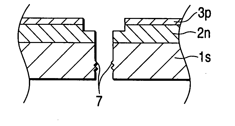
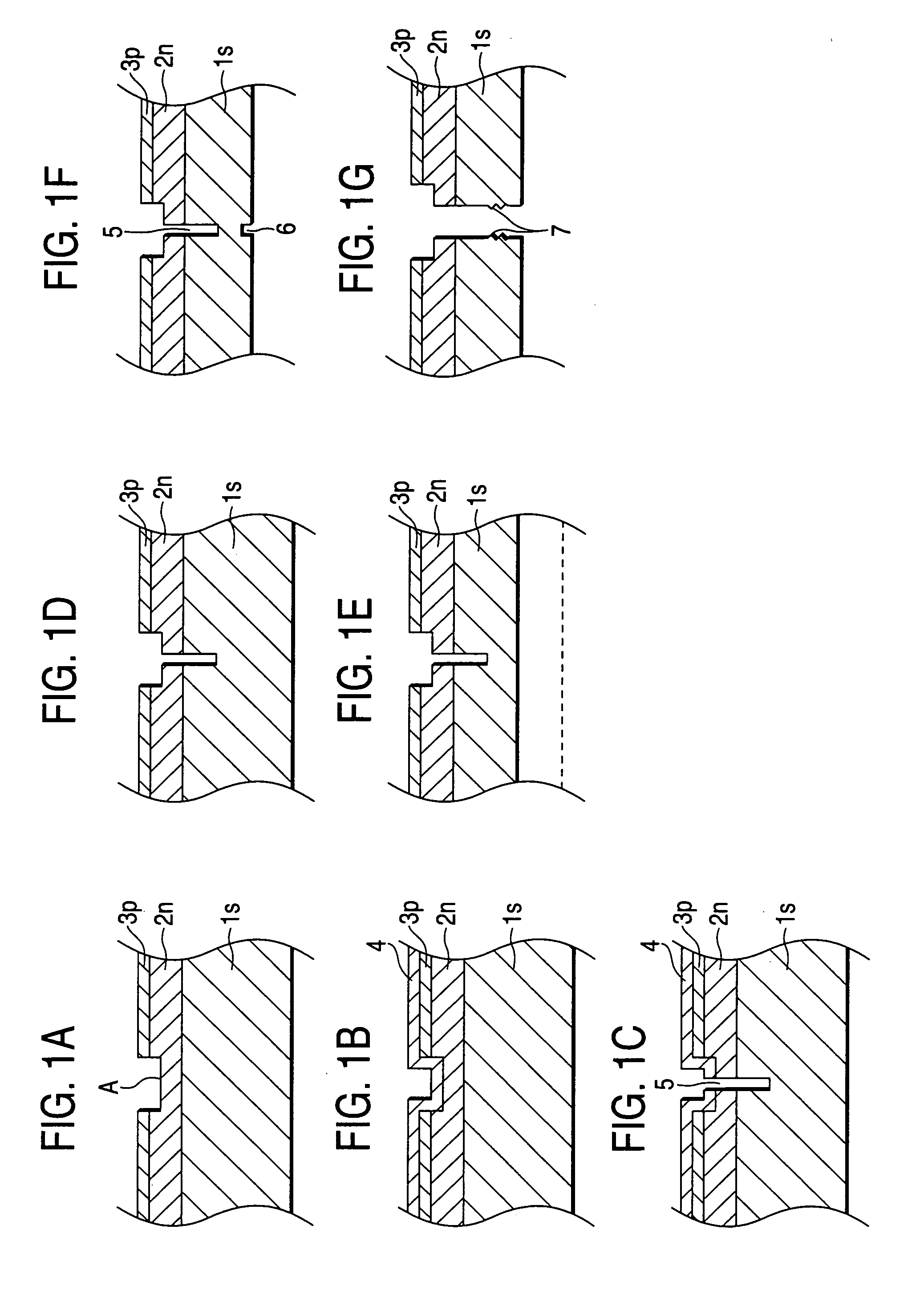
[0108]FIGS. 1A to 1G are step views (sectional views) for explaining a first embodiment of the invention. A plurality of Group III nitride compound semiconductor layers are formed on a substrate 1s for performing the formation of elements and the formation of electrodes. Although two Group III nitride compound semiconductor layers 2n and 3p are shown representatively in each of FIGS. 1A to 1G, the two layers 2n and 3p mean layers which must not be short-circuited and do not mean the fact that only two Group III nitride compound semiconductor layers are provided. Then, a state in which only the electrode-forming layer on a side near the substrate is left is formed on each parting line by etching or dicing due to a dicer (FIG. 1A). That is, concave portions A are formed. Here, the term “parting lines” means latticed frame-shaped lines in the case where ideal parting surfaces (perpendicular to the substrate is surface) for dividing the substrate 1s into individual Group III nitride com...

second embodiment

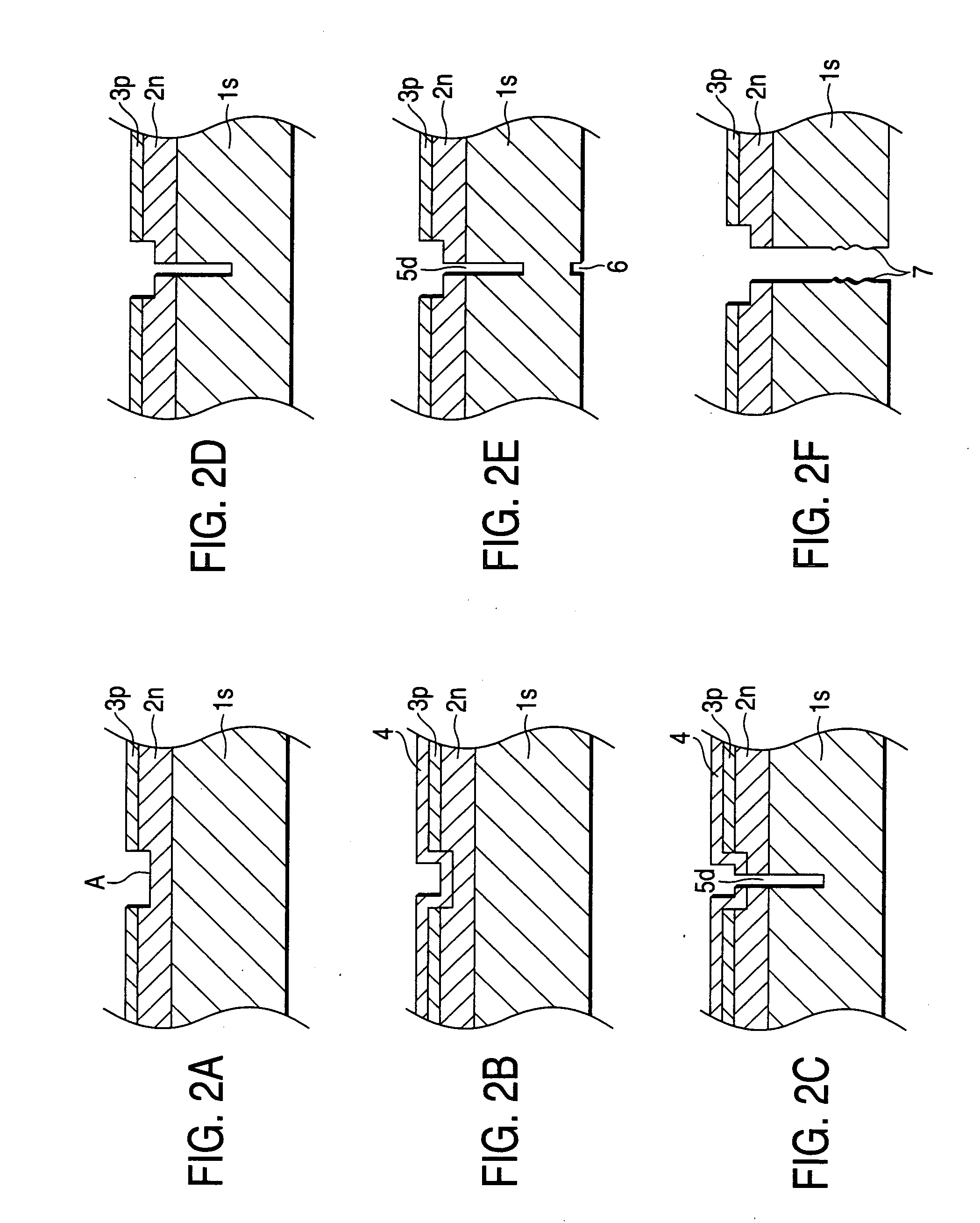
[0111]FIGS. 2A to 2F are step views (sectional views) for explaining a second embodiment of the invention. A state in which only the electrode-forming layer on a side near the substrate is left is formed on the parting lines by etching or dicing due to a dicer in the same manner as in the first embodiment shown in FIGS. 1A to 1G (FIG. 2A) In this case, it is a matter of course that etching or dicing due to a dicer may be performed until the substrate 1s is exposed or part of the front surface of the substrate 1s is removed. Then, a protective film 4 which can be removed by an after-process is formed on the whole front surface (FIG. 2B). Then, in this embodiment, first grooves 5d with a depth of not smaller than about ⅕ as large as the thickness of the substrate is are formed like a latticed frame in the front surface side (element-forming side) of the substrate 1s along the latticed frame-shaped parting lines (FIG. 2C). Then, the protective film 4 is removed together with reaction p...

third embodiment

[0113]FIGS. 3A to 3F are step views (sectional views) for explaining a third embodiment of the invention. A state in which only the electrode-forming layer on a side near the substrate is left is formed on the parting lines by etching or dicing due to a dicer in the same manner as in the second embodiment shown in FIGS. 2A to 2F (FIG. 3A). In this case, it is a matter of course that etching or dicing due to a dicer may be performed until the substrate 1s is exposed or part of the front surface of the substrate 1s is removed. Then, a protective film 4 which can be removed by an after-process is formed on the whole front surface (FIG. 3B). Then, first grooves 5d with a depth not smaller than the thickness of the thin-walled substrate 1s which will be polished by an after-process are formed like a latticed frame in the front surface side (element-forming side) of the substrate 1s along the latticed frame-shaped parting lines (FIG. 3C). Then, the protective film 4 is removed together wi...


PUM

PropertyMeasurementUnit
depthaaaaaaaaaa
thicknessaaaaaaaaaa
thicknessaaaaaaaaaa

Abstract

A plurality of Group III nitride compound semiconductor layers are formed on a substrate for performing the formation of elements and the formation of electrodes. The Group III nitride compound semiconductor layers on parting lines are removed by etching or dicing due to a dicer so that only an electrode-forming layer on a side near the substrate remains or no Group III nitride compound semiconductor layer remains on the parting lines. A protective film is formed on the whole front surface. Separation grooves are formed in the front surface of the substrate by laser beam irradiation. The protective film is removed together with reaction products produced by the laser beam irradiation. The rear surface of the substrate 1s is polished to reduce the thickness of the substrate. Then, rear grooves corresponding to the latticed frame-shaped parting lines are formed in the rear surface of the substrate. The substrate is divided into individual elements along the parting lines.

Description

[0001] The present application is based on Japanese Patent Applications No. 2002-183730, 2002-326194, 2002-326195 and 2003-013398, which are incorporated herein by reference. BACKGROUND OF THE INVENTION [0002] 1. Field of the Invention [0003] The present invention relates to a method for producing a semiconductor element formed on a substrate. Particularly, the invention relates to a method for obtaining semiconductor elements with a good yield by individually dividing the semiconductor elements formed on a substrate in an easy way. [0004] 2. Description of the Related Art [0005] In production of a Group III nitride compound semiconductor element such as an LED, sapphire, spine 1 or the like is used as a substrate material. Substrates made of these materials differ from substrates using silicon and gallium arsenide in that they are not easy to process. Accordingly, when a wafer obtained by lamination of Group III nitride compound semiconductors on a substrate made of one of these ma...

Claims


Application Information

Patent Timeline
Patent Type & Authority Applications(United States)
IPC IPC(8): B23K26/40H01L21/301H01L21/78H01L33/00H01L33/32H01S5/02H01S5/323
CPCB23K26/18B23K26/367B23K26/4075B23K26/409B23K2201/40B23K26/009H01L33/0095H01L33/32H01S5/0201H01S5/32341H01L21/78B23K26/40B23K26/364B23K2101/40B23K2103/172B23K2103/50H01L21/30
Inventor HASHIMURA, MASAKIKONISHI, SHIGEKINAGASAKA, NAOHISA
Owner TOYODA GOSEI CO LTD
Why Eureka
Try Eureka