

Via structure of packages for high frequency semiconductor devices
a technology of high-frequency semiconductors and via structures, applied in the direction of high-frequency circuit adaptations, electrical apparatus construction details, printed circuit aspects, etc., can solve the problems of inability to provide impedance matching through conventional via structures, inability to preserve clean signals without mutual interference, and inability to provide impedance matching. conventional structures, to achieve the effect of increasing enhancing the capacitance of vias, and high i/o counts
- Summary
- Abstract
- Description
- Claims
- Application Information
AI Technical Summary
Benefits of technology
Problems solved by technology
Method used
Image

Examples
Embodiment Construction
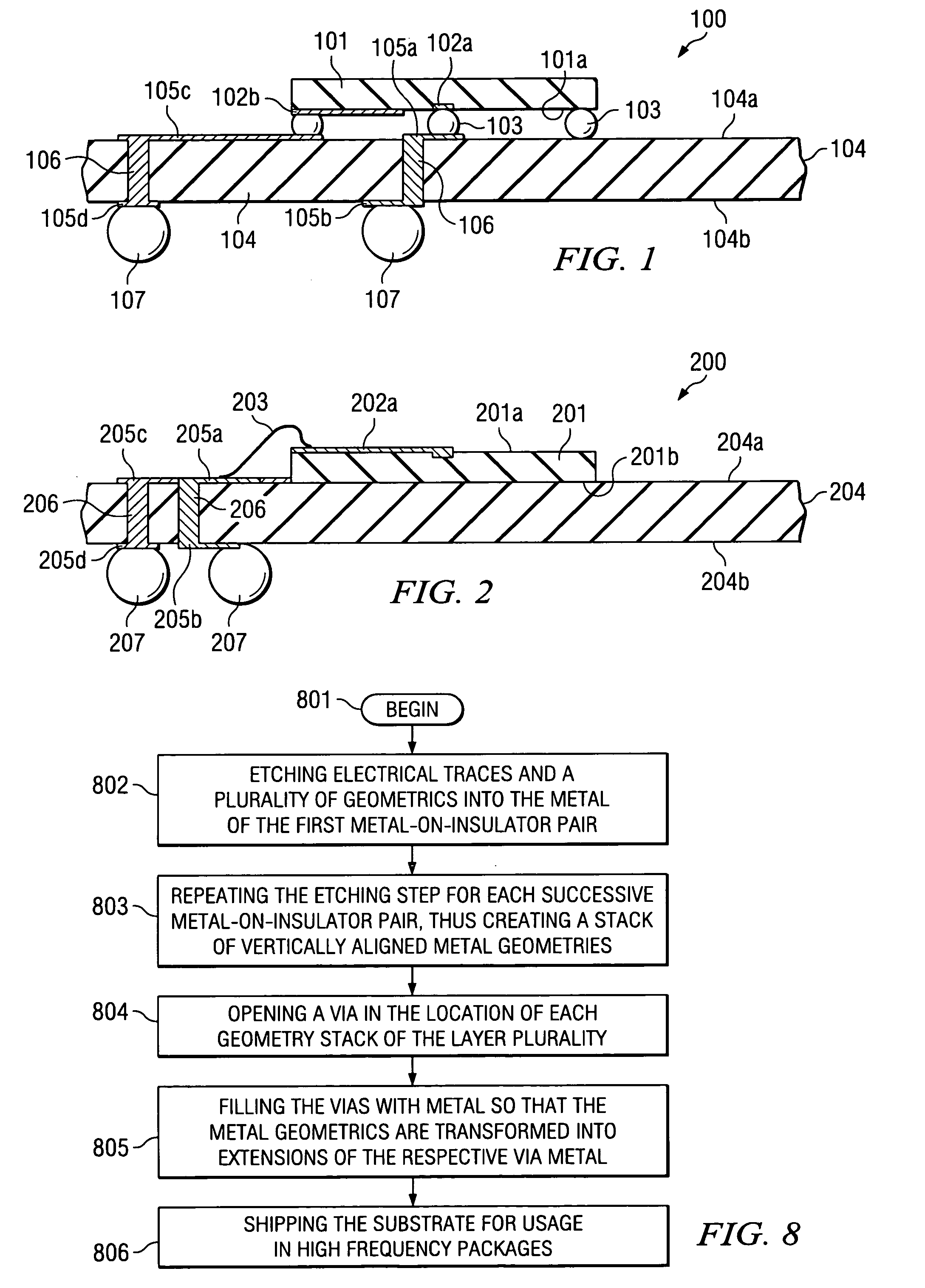
[0023]FIGS. 1 and 2 depict schematically cross sections through semiconductor devices generally designated 100 and 200, respectively. The devices consist of a semiconductor chip 101 and 201, respectively, having an integrated circuit on its active surface 101a and 201a, respectively. The semiconductor material of chip 101 or 102 may be silicon, silicon germanium, gallium arsenide, or any other semiconductor material. In FIG. 1, the active surface has a plurality of bond pads 102a, 102b, etc. and an interconnection element 103 attached to each bond pad. In FIG. 2, a bond pad 202a is shown suitable for connection by means of a bonding wire 203.
[0024] In FIGS. 1 and 2, the devices 100 and 200 further include a substrate 104 and 204, respectively. The substrates are made of insulating material, for example ceramic or plastic such as FR-4. The substrates have first and second surfaces, 104a and 104b, respectively, in FIGS. 1 and 204a and 204b, respectively, in FIG. 2. On each surface, t...
PUM
 Abstract
Description
Claims
Application Information