Circuit and method for broadband switching noise suppression in multilayer printed circuit boards using localized lattice structures

a multi-layer printed circuit board and broadband switching technology, applied in cross-talk/noise/interference reduction, printed capacitor incorporation, printed element electric connection formation, etc., can solve the problems of l(di/dt) noise that can be substantial, power plane noise induced in the power distribution system, power plane noise induced in the ground plane, etc., to achieve the effect of suppressing digital noise on the power plane, eliminating power plane resonance, and improving rf isolation

Inactive Publication Date: 2005-09-22
ETENNA
View PDF25 Cites 125 Cited by
  • Summary
  • Abstract
  • Description
  • Claims
  • Application Information

AI Technical Summary

Benefits of technology

[0009] By way of introduction only, the present embodiments provide periodic conductive structures which act as distributed microwave bandstop filters integrated into parallel-plate waveguides. These embodiments can be used as electromagnetic interference (EMI) filters to suppress digital noise on power planes, as well as to eliminate power ...

Problems solved by technology

A common problem in electronic systems is switching noise induced in the power distribution system by switching of digital circuits of the system.
If the system includes digital or other circuits with fast-switching outputs, noise can be induced in the power planes and even in the ground plane.
Another noise mechanism is the internal short-circuit current that occurs within the digital circuits, which can reach several Amperes producing low impedance—high impulse transitions of various frequencies which progress through the power planes.
The noise may have several sources, but generally is due to the high slew rate of the digital output and the non-zero inductance of the power plane.
Especially for an output driving a large capacitive load, the L(di/dt) noise can be substantial.
This noise on the power plane can affect other circuits, slowing system operation or producing data errors.
The problem occurs in all types of systems, including integrated circuits and circuits formed on pr...

Method used


Image

  • Circuit and method for broadband switching noise suppression in multilayer printed circuit boards using localized lattice structures
  • Circuit and method for broadband switching noise suppression in multilayer printed circuit boards using localized lattice structures
  • Circuit and method for broadband switching noise suppression in multilayer printed circuit boards using localized lattice structures

Examples


first embodiment

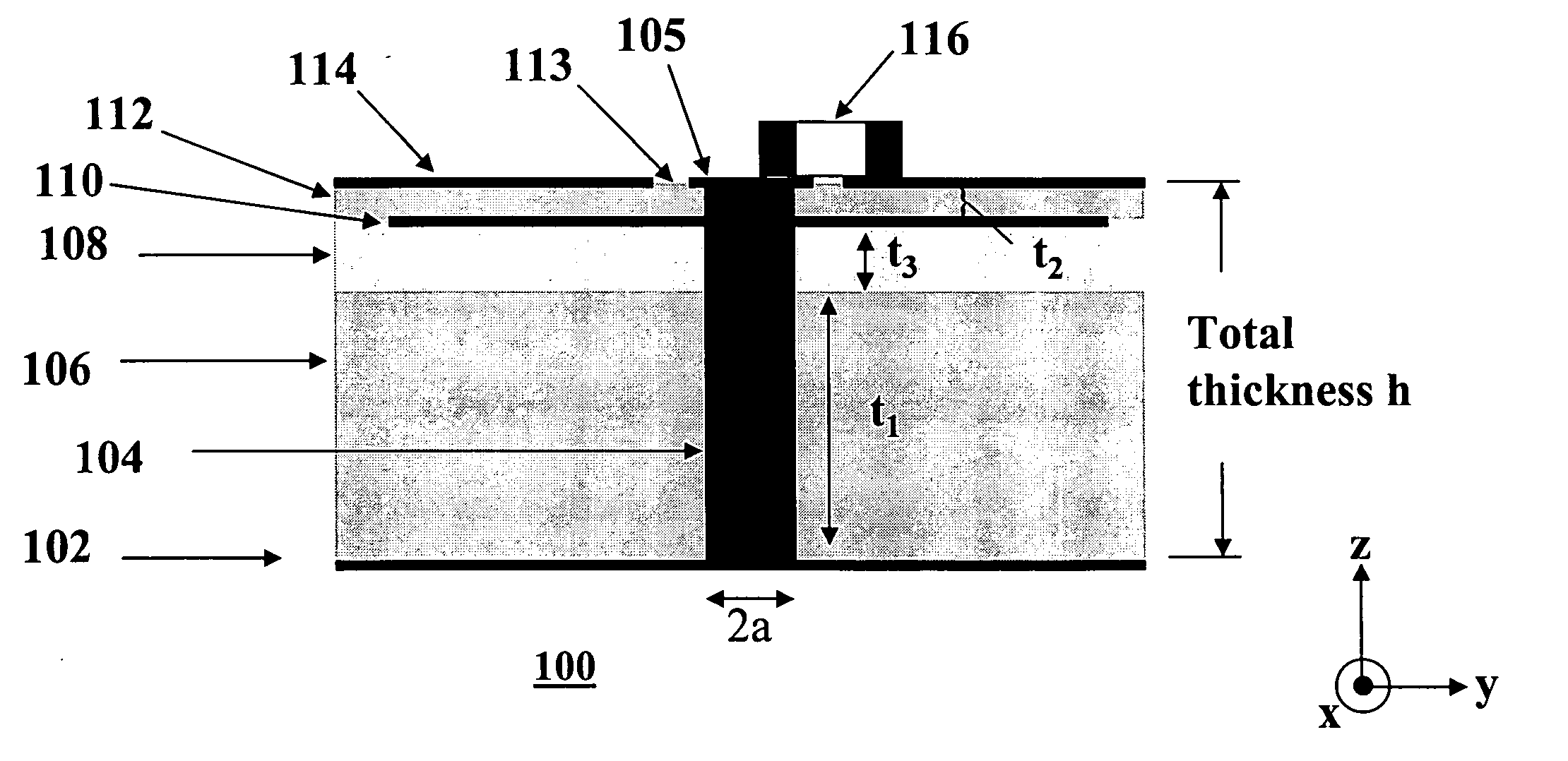
[0041] Referring now to the drawings, FIG. 1 illustrates a parallel plate waveguide (PPW) 100 containing a transverse electromagnetic (TEM) mode suppression circuit. FIG. 1 is a cross-sectional view of the PPW 100. The PPW 100 includes a lower metal layer 102, an upper metal layer 114 separated by three dielectric regions. An array of conductive rods 104 of length h and radius a extends through all three dielectric layers from lower metal layer 102 to the upper metal layer 114. A bonding film 108 of thickness t3 is disposed between the first dielectric layer 106 of thickness t1 and the second dielectric layer 112 of thickness t2. Buried patches are contained in a third metal layer 110 between the second dielectric layer 112 and the third dielectric layer 108 which is the bonding film and make contact with the vias 104. Unless otherwise noted, the dimensions shown in the figures do not include the thickness of the conductive surfaces, which may be a relatively thin metal. The conduct...

embodiment 326

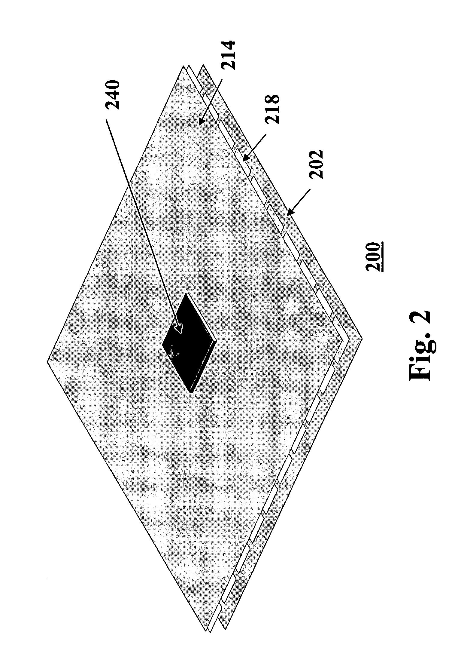
[0051] Patches can completely surround an open central region and change in size with distance from the central region. Inhomogeneous mode suppression structures may be created to allow broader frequency stopbands between two different reference plane locations on the same PCB. In these structures, the stopband edges vary in frequency as a function of lateral position within the PCB because the properties of the unit cell change with location. One example of such a structure is shown in embodiment 326 of FIG. 3. In this embodiment, the patches decrease in size from the central region 332. The array of patches contains larger patches 334, and smaller patches 336. As mentioned, these different patch and unit cell sizes attenuate the electromagnetic waves within different frequency regions. Although only 2 unit cells of each type of patch are shown, more unit cells or fewer unit cells may be present. In addition, although the patch size shown in FIG. 3 decreases with increasing distanc...

embodiment 322

[0070] Now we turn to experimental results of localized arrays of patches and capacitors. Experiments were performed to test the actual frequency response of different types of arrangements: those in which the arrays of patches and / or chip capacitors extend throughout the PCB and those with localized arrays. A top view of a parallel plate waveguide with 5×5 arrays of buried patches around ports 2 and 3 is shown in FIG. 16. Pads are available for SMT capacitors to be mounted. However, there are no SMT capacitors mounted on the board in this figure. The PCB is of dimensions 4.25 inches by 5.25 inches. The patches are squares having 230 mils side dimension and a spacing of 20 mils between the patches. The stackup of this board is the same as that shown in FIG. 1. The dielectric layer between the patches and the bottom layer is 24 mils thick and has a relative dielectric constant of 2.5, the dielectric layer between the patches and the top layer is 3 mils thick and has a relative dielec...


PUM


Abstract

An apparatus for suppressing noise in an electronic device includes a multiple layer structure in which localized arrays of chip capacitors and/or patches around sources of electromagnetic waves are used. The PCB includes multiple conductive layers at different potentials, dielectric layers separating the conductive layers, conductive rods extending between at least two of the conductive layers, and a layer of patches disposed adjacent or on one or more of the conductive layers. The conductive rods are connected to one of the conductive layers and chip capacitors connect the conductive rods to another of the conductive layers. A particular location can be effectively isolated from noise using a few unit cells of an array of patches/capacitors partially or completely surrounding the particular location.

Description

BACKGROUND [0001] This invention is related generally to reduction of noise induced in power planes due to switching of digital circuits. More particularly, the present invention is related to circuits and methods for suppression of transverse electromagnetic modes in parallel plate waveguides. [0002] A common problem in electronic systems is switching noise induced in the power distribution system by switching of digital circuits of the system. Conventionally, such a system has one or more power planes designated, for example, +Vcc, and one or more ground planes. The potential difference between the power plane and the ground plane provides operating voltage for the circuits of the system. If the system includes digital or other circuits with fast-switching outputs, noise can be induced in the power planes and even in the ground plane. Another noise mechanism is the internal short-circuit current that occurs within the digital circuits, which can reach several Amperes producing low...

Claims


Application Information

Patent Timeline
IPC IPC(8): H05K1/02H05K1/11H05K1/16H05K3/42H05K7/06H05K9/00
CPCH05K1/0231H05K1/0236H05K1/116H05K1/162H05K3/429H05K2201/09781H05K2201/0191H05K2201/09481H05K2201/09618H05K2201/09672H05K2201/09681H05K9/0039
Inventor ROGERS, SHAWN D.STEIGERWALD, TODD
Owner ETENNA
Why Eureka
Try Eureka