Method of removing resist, semiconductor device thereby and method of manufacturing a semiconductor device

a technology of semiconductor devices and resists, which is applied in the field of methods of removing resists, semiconductor devices thereby and methods of manufacturing semiconductor devices, can solve problems such as the decrease of the processing speed of ics, and achieve the effect of high repeatability and accuracy, potentially and effectively applicable to manufactur

Inactive Publication Date: 2005-09-22
SONY CORP
View PDF14 Cites 29 Cited by
  • Summary
  • Abstract
  • Description
  • Claims
  • Application Information

AI Technical Summary

Benefits of technology

[0013] Application of the resist removal method by this invention enables to form a low dielectric constant ILD for wiring structure of semiconductor devices conveniently in high repeatability and accuracy. Resist removing by use of hydrogen gas realizes complete removal of resist, leaving none of residue. The invention presents the method of resist removing by hydrogen gas, which method is potentially and effectively applicable to manufacture of semiconductor devices.

Problems solved by technology

Particularly in manufacturing logic integrated circuits (ICs), a problem is decrease of processing speed of ICs caused by increase of resistance and increase of parasitic capacitance as a result of microscopic wiring onto the ILD.

Method used


Image

  • Method of removing resist, semiconductor device thereby and method of manufacturing a semiconductor device
  • Method of removing resist, semiconductor device thereby and method of manufacturing a semiconductor device
  • Method of removing resist, semiconductor device thereby and method of manufacturing a semiconductor device

Examples


embodiment 1

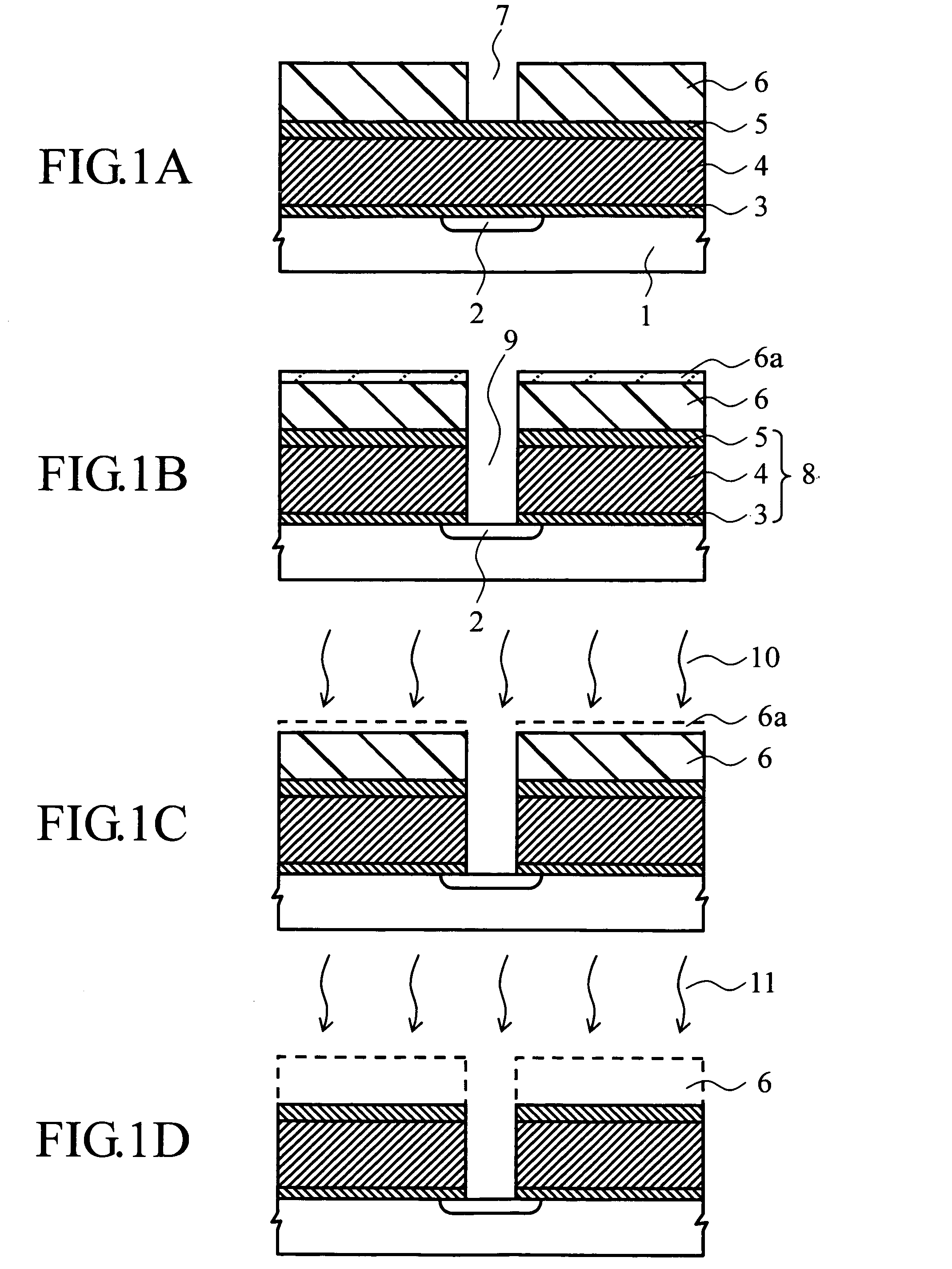
[0032]FIG. 1A-1D,FIG. 2A-2C and FIG. 3A-3C describe process-wise cross sectional views of a substrate with an ILD and a protection film and a resist mask thereon to explain the example of embodying this invention.

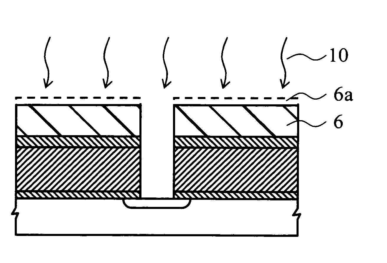
[0033] Firstly an n-conductive diffusion layer 2 is formed on the surface of a p-conductive silicon substrate 1, and on the surface of the same substrate a silicon oxide film 3 of 50 nm thickness, for instance, by thermal oxidation. Then, on the silicon oxide film 3, a MSQ film 4 of approximate 1.5 μm is made by widely known spin-on coating method. And, laminating a SiC film 50 nm thick on the MSQ film 4, a protection insulating film 5 is formed. Further, a resist mask 6 is made on the protection insulating film 5 on the substrate by photolithography technology. An opening 7 is formed on the resist mask 6. (FIG. 1A).

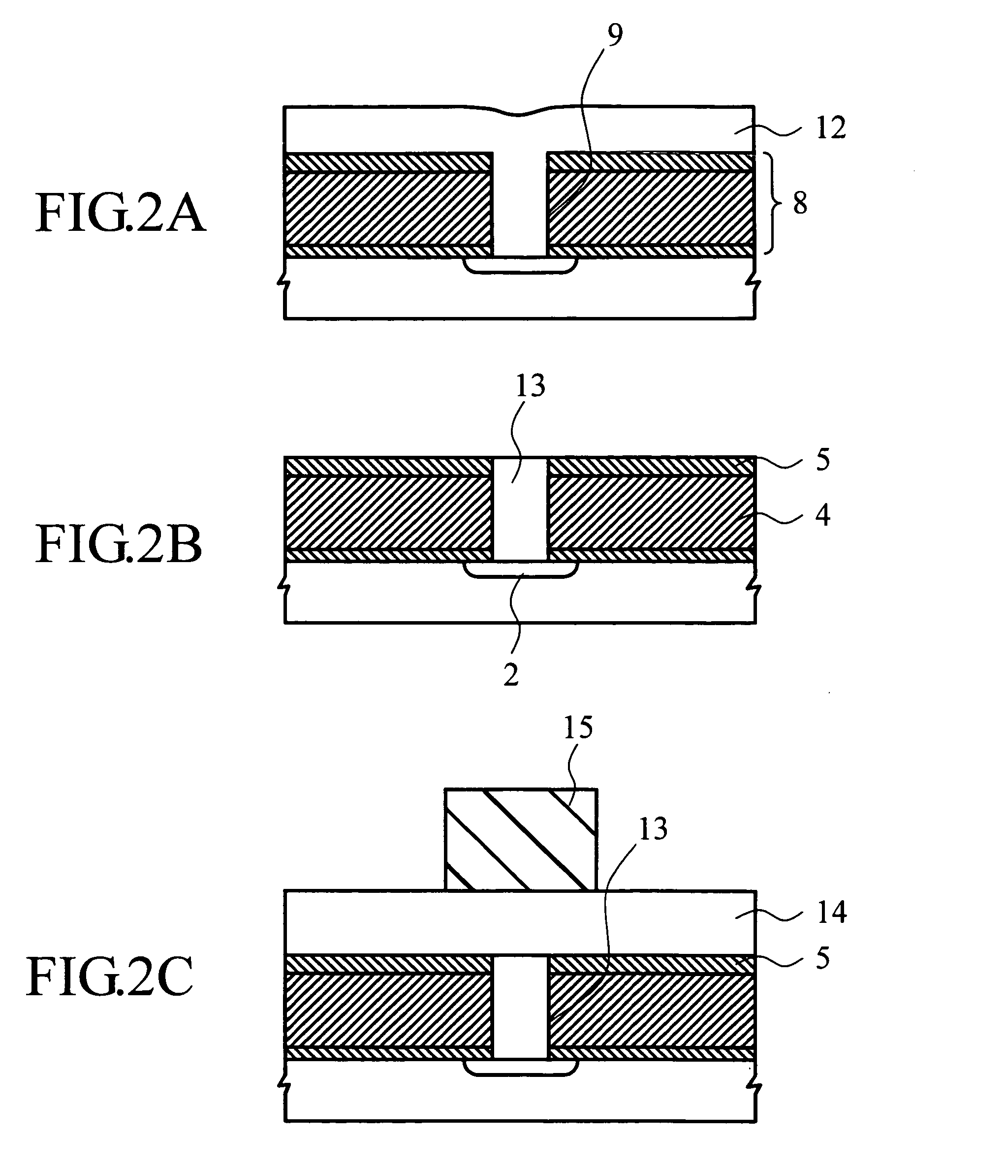
[0034] Next, as explained in the above referring to conventional technology, an ILD 8 consisting of the protection insulating film 5, the MSQ film 4, and the ...

embodiment 2

[0056]FIG. 7A-7C and FIG. 8A-8C depict process-wise cross sectional views of a semiconductor device to which applied is a resist removing method in the example 2 of embodying this invention. The example 2 is the case of forming dual damascene wiring structure.

[0057] Firstly, on the surface of a silicon substrate (drawing not shown) formed is a base insulating film 51 of silicon oxide film; on the base insulating film 51 formed is 1st barrier layer 52 of titanium-related conductive material; on the layer 52, a lower wiring layer 53 of aluminum and copper alloy film; on the layer 53, 2nd barrier layer 54, four layers in laminate. Then, solution which is to be a MSQ film is coated over the whole surface by spin-on coating method, and then the substrate with four films thereon is sintered in temperature of about 150° C., for instance, and moreover, by heat treatment in about 400° C. in a diffusion furnace, 1st MSQ film 55 is formed in about 500 nm thickness. Subsequently, on the surfac...


PUM

PropertyMeasurementUnit
temperatureaaaaaaaaaa
thickaaaaaaaaaa
thicknessaaaaaaaaaa

Abstract

Disclosed is a method of removing resist preventing increase of dielectric constant of low permittivity insulating films and preventing remains of resist. Using a resist mask, a protection insulating film, a MSQ film, and a silicon oxide film composing an ILD are RIE dry etched sequentially, and a via is formed on the surface of a substrate for processing reaching the diffusion layer on the substrate for processing. Subsequent process consists of; removing a modified layer formed on the substrate for processing surface because of prior etching using plasma gas by plasma excitation of NH3 gas, and another etching for complete removal of the resist mask by irradiation of hydrogen active species created by hydrogen gas and inert gas, of which example is helium gas or argon gas.

Description

TECHNICAL FIELD [0001] This invention relates to method of removing resist, semiconductor device thereby and method of manufacturing a semiconductor device using the method of removing resist. More particularly but not exclusively, the invention relates to a method, in removing the film of resist coated onto a substrate, to prevent rising of dielectric constant of an inter-layer dielectric (ILD) which consists of low dielectric constant insulating film materials, and a method to remove resist completely without leaving residue. The invention also involves semiconductor device manufactured according to the method. BACKGROUND OF THE INVENTION [0002] Today, semiconductor manufacturing especially of a very large scale integrated circuit (VLSI) that is formed on a silicon substrate, indispensably entails micro fabrication of elements or circuit components and forming multilayer interconnect wiring to bond the elements. As operation at lower voltages and higher processing speed are requir...

Claims


Application Information

Patent Timeline
Patent Type & Authority Applications(United States)
IPC IPC(8): H01L21/3065G03F7/42H01L21/027H01L21/311H01L21/3213H01L21/461H01L21/4763H01L21/768
CPCG03F7/427H01L21/0274H01L21/7681H01L21/31144H01L21/76802H01L21/31138
Inventor MATSUSHITA, ATSUSHIMATSUMOTO, ISAOINUKAI, KAZUAKISHIN, HONG JAEOHASHI, NAOFUMISONE, SHUJIMISAWA, KAORI
Owner SONY CORP
Why Eureka
Try Eureka