
Method and system for treating a dielectric film

Inactive Publication Date: 2005-09-29
TOKYO ELECTRON LTD
View PDF5 Cites 73 Cited by
  • Summary
  • Abstract
  • Description
  • Claims
  • Application Information

AI Technical Summary

Benefits of technology

[0009] One aspect of the present invention is to reduce or eliminate any of the above-described problems or other problems in the prior art relating to processing dielectric films.
[0011] Yet another aspect of the present invention is to treat a dielectric film in order to reduce diffusion of barrier material into the dielectric film and / or improve adhesion of the barrier film to the dielectric film.

Problems solved by technology

As is known to those in the semiconductor art, interconnect delay is a major limiting factor in the drive to improve the speed and performance of integrated circuits (IC).
While low-k materials are promising for fabrication of semiconductor circuits, the present inventors have recognized that these films also provide many challenges.
First, low-k films tend to be less robust than more traditional dielectric layers and can be damaged during wafer processing, such as by etch and plasma ashing processes generally used in patterning the dielectric layer.
Further, some low-k films tend to be highly reactive when damaged, particularly after patterning, thereby allowing the low-k material to absorb water and / or react with other vapors and / or process contaminants that can alter the electrical properties of the dielectric layer.
However, exposure of the pores and / or damage of the low-k film following the etching of patterns in the dielectric film causes problems with diffusion of the barrier material and copper through imperfections in the barrier film local to these exposed pores, as well as poor adhesion of the barrier layer to the dielectric film.
Additionally, porous low-k dielectric films, such as the damaged low-k films noted above, are susceptible to absorbing moisture, and other contaminants.

Method used


Image

  • Method and system for treating a dielectric film
  • Method and system for treating a dielectric film
  • Method and system for treating a dielectric film

Examples


Embodiment Construction

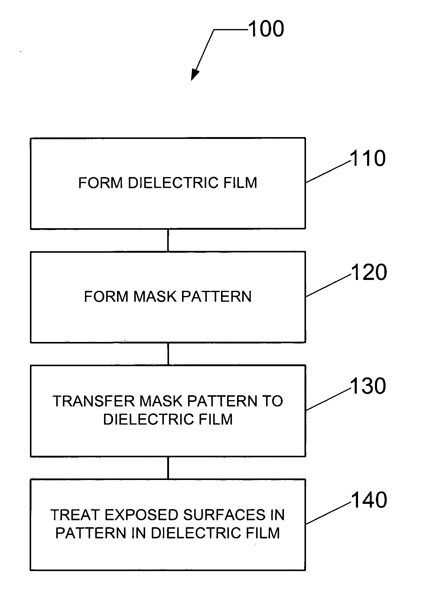
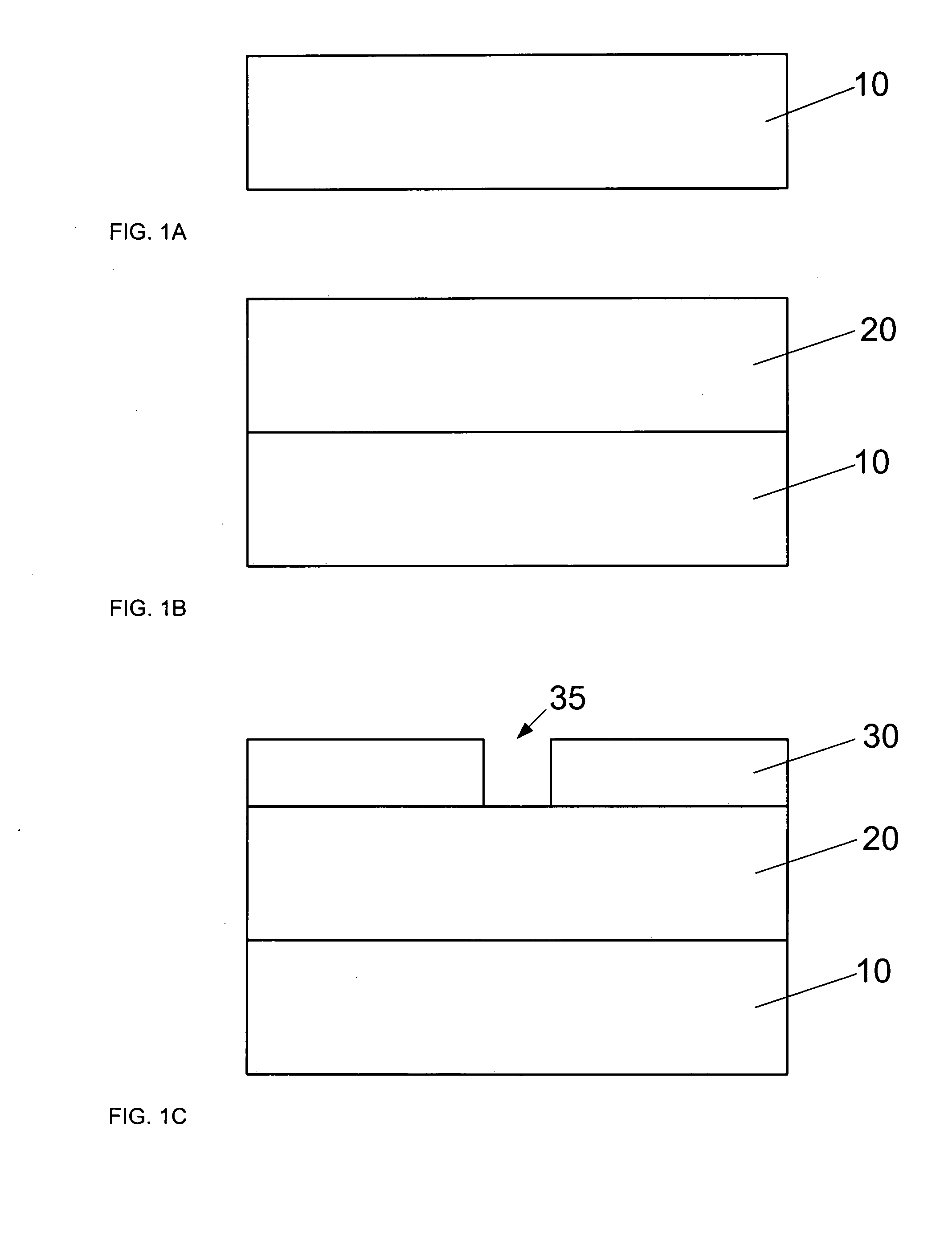
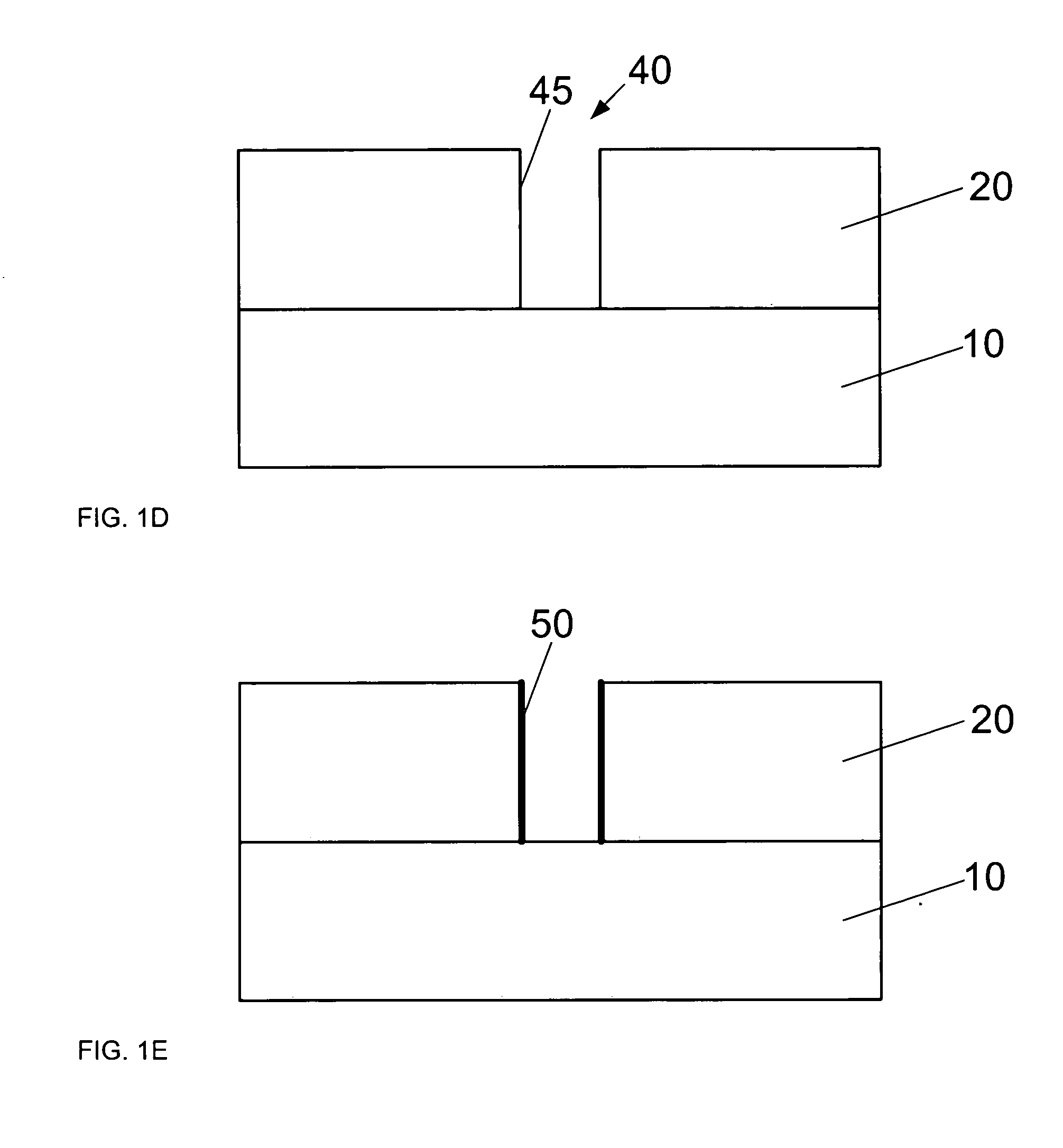
[0027] Referring now to the drawings, wherein like reference numerals designate identical or corresponding parts throughout the several views, FIGS. 1A through 1E present a schematic representation of a method of forming a pattern in a dielectric film and treating the exposed surfaces of the etched pattern in the dielectric film in order to perform at least one of healing, sealing, and cleaning these surfaces. Additionally, FIG. 2 presents a flow chart 100 of performing the method according to an embodiment of the present invention. As shown in FIGS. 1A, 1B, and 2, a dielectric film 20 is formed in 110 on an upper surface of a substrate 10 that may or may not include additional layers. The substrate 10 may be a semiconductor, a metallic conductor, or any other substrate to which the dielectric film is to be formed upon. The dielectric film has a nominal dielectric constant value less than the dielectric constant of SiO2, which is approximately 4 (e.g., the dielectric constant for th...


PUM


Abstract

A method and system for treating a dielectric film includes exposing at least one surface of the dielectric film to an alkyl silane, an alkoxysilane, an alkyl siloxane, an alkoxysiloxane, an aryl silane, an acyl silane, a cyclo siloxane, a polysilsesquioxane (PSS), an aryl siloxane, an acyl siloxane, or a halo siloxane, or any combination thereof. The dielectric film can include a low dielectric constant film with or without pores having an etch feature formed therein following dry etch processing. As a result of the etch processing or ashing, exposed surfaces in the feature formed in the dielectric film can become damaged, or activated, leading to retention of contaminants, absorption of moisture, increase in dielectric constant, etc. Damaged surfaces, such as these, are treated by performing at least one of healing these surfaces to, for example, restore the dielectric constant (i.e., decrease the dielectric constant) and cleaning these surfaces to remove contaminants, moisture, or residue. Moreover, preparation for barrier layer and metallization of features in the film may include treating by performing sealing of sidewall surfaces of the feature to close exposed pores and provide a surface for barrier film deposition.

Description

CROSS-REFERENCE TO RELATED APPLICATIONS [0001] This application is related to co-pending U.S. patent application Ser. No. 10 / 682,196, entitled “Method and system for treating a dielectric film”, Attorney docket no. 243414US, filed on Oct. 10, 2003, the content of which is incorporated by reference in its entirety.BACKGROUND OF THE INVENTION [0002] 1. Field of the Invention [0003] The present invention relates to a method and system for treating a dielectric film and, more particularly, to a method and system of treating a dielectric film in order to perform at least one of healing, sealing, and cleaning the dielectric film. [0004] 2. Description of Related Art [0005] As is known to those in the semiconductor art, interconnect delay is a major limiting factor in the drive to improve the speed and performance of integrated circuits (IC). One way to minimize interconnect delay is to reduce interconnect capacitance by using low dielectric constant (low-k) materials during production of ...

Claims


Application Information

Patent Timeline
IPC IPC(8): H01L21/311H01L21/316H01L21/768H01L23/532
CPCH01L21/02063H01L21/02101H01L21/02126H01L21/02337H01L21/3105H01L23/5329H01L21/31695H01L21/76802H01L21/76814H01L21/76826H01L21/76831H01L21/31633H01L2924/0002H01L21/02274H01L21/02282H01L21/02203H01L21/02216H01L2924/00
Inventor KEVWITCH, ROBERTHANSEN, BRANDONTOMA, DOREL IOANZHU, JIANHONG
Owner TOKYO ELECTRON LTD
Learn More