Integrated circuit device
- Summary
- Abstract
- Description
- Claims
- Application Information
AI Technical Summary
Benefits of technology
Problems solved by technology
Method used
Image

Examples
Embodiment Construction
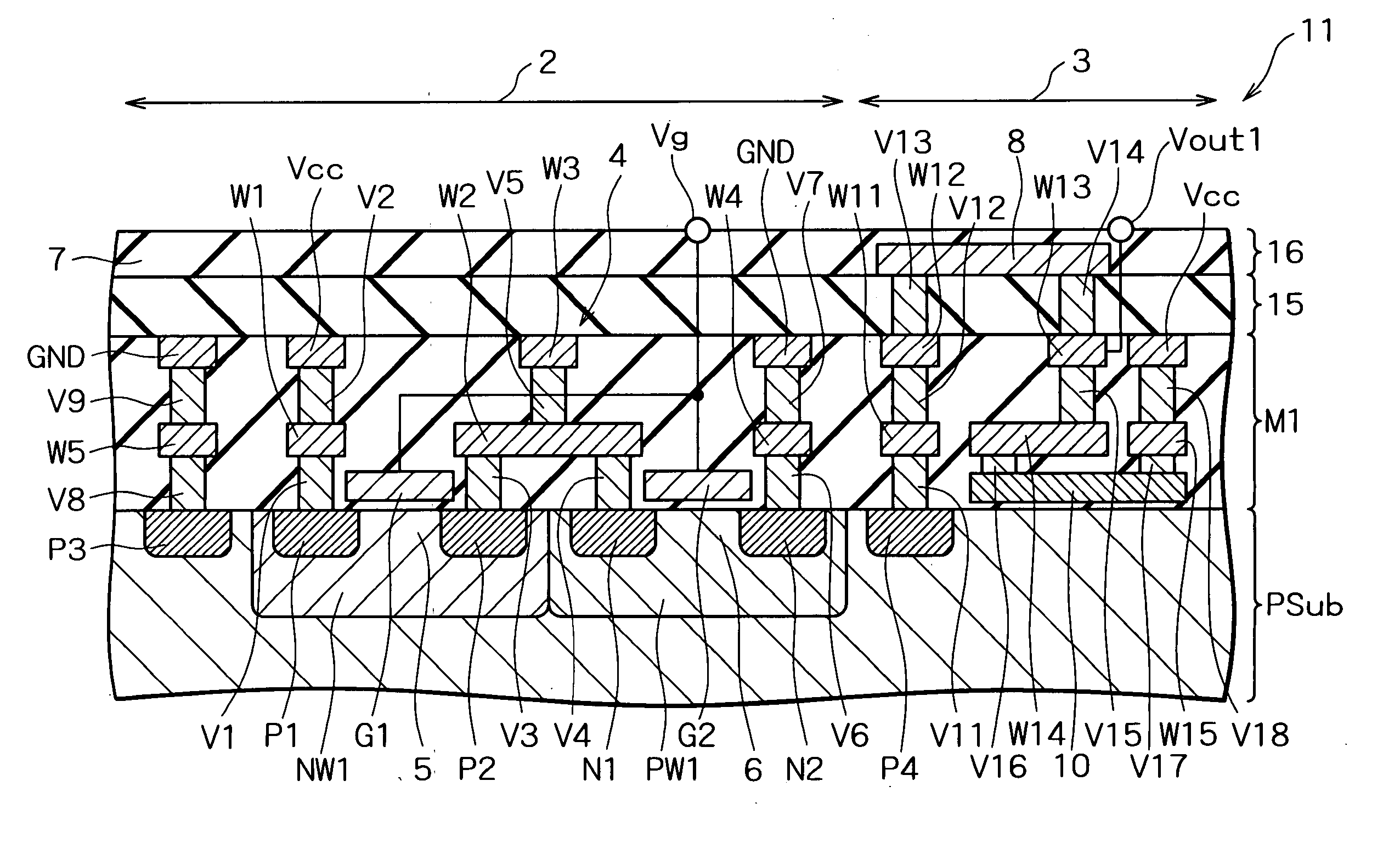
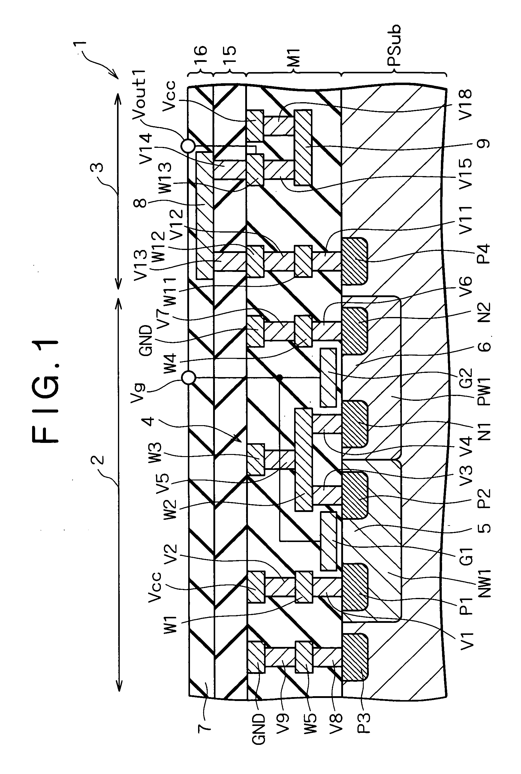
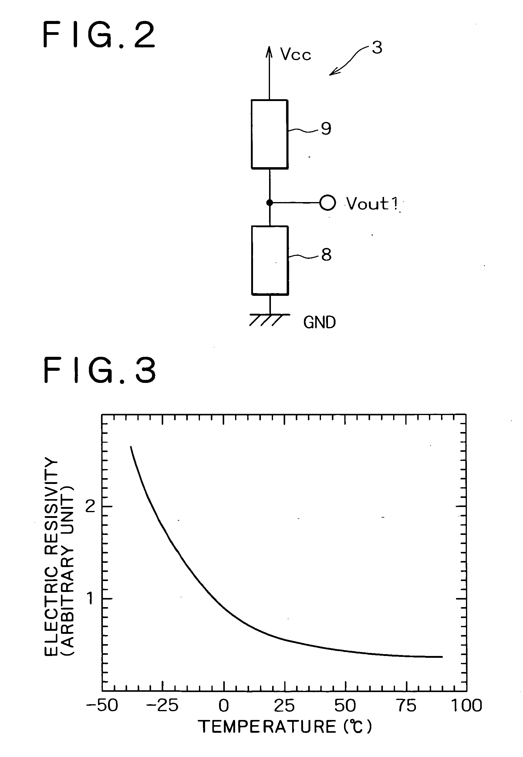
[0024] Preferred embodiments of the present invention will be described specifically below with reference to the accompanying drawings. To begin with, the first embodiment of the invention will be discussed. FIG. 1 is a cross-sectional view showing a semiconductor integrated circuit device according to a first embodiment of the present invention, and FIG. 2 is an equivalent circuit diagram showing the temperature sensor section of the semiconductor integrated circuit device shown in FIG. 1. FIG. 3 is a graph showing the temperature dependence of the electric resistivity of vanadium oxide, showing the temperature on the abscissa and the electric resistivity of vanadium oxide on the ordinate. The semiconductor integrated circuit device according to the embodiment is formed on a single silicon chip.
[0025] As shown in FIG. 1, the semiconductor integrated circuit device 1 of the embodiment includes a P-type silicon substrate PSub, a multi-layer wiring layer M1 formed on the P-type silic...
PUM
 Abstract
Description
Claims
Application Information
 - R&D
- Intellectual Property
- Life Sciences
- Materials
- Tech Scout
- Unparalleled Data Quality
- Higher Quality Content
- 60% Fewer Hallucinations
Browse by: Latest US Patents, China's latest patents, Technical Efficacy Thesaurus, Application Domain, Technology Topic, Popular Technical Reports.
© 2025 PatSnap. All rights reserved.Legal|Privacy policy|Modern Slavery Act Transparency Statement|Sitemap|About US| Contact US: help@patsnap.com