

Optical integrated device
a technology of integrated devices and optical components, applied in the field of optical devices, can solve the problems of reducing the carrier confinement into the active region, degrading the device's performance against temperature, and inevitably induced reflection of light at the interfa
- Summary
- Abstract
- Description
- Claims
- Application Information
AI Technical Summary
Benefits of technology
Problems solved by technology
Method used
Image

Examples
first embodiment
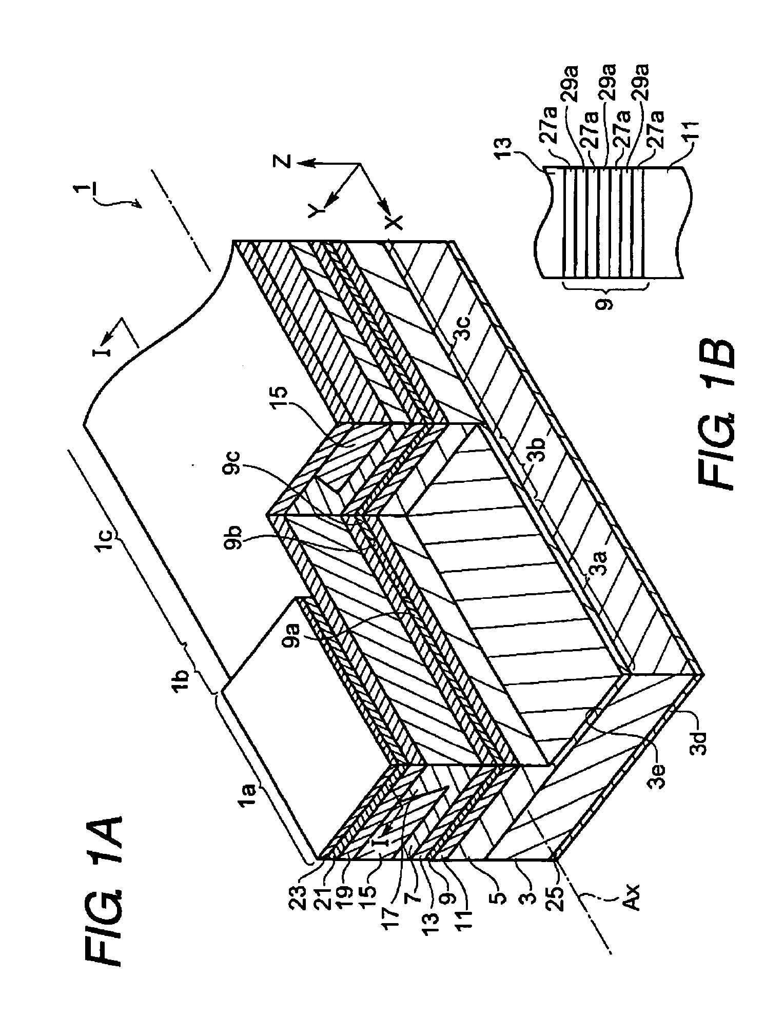
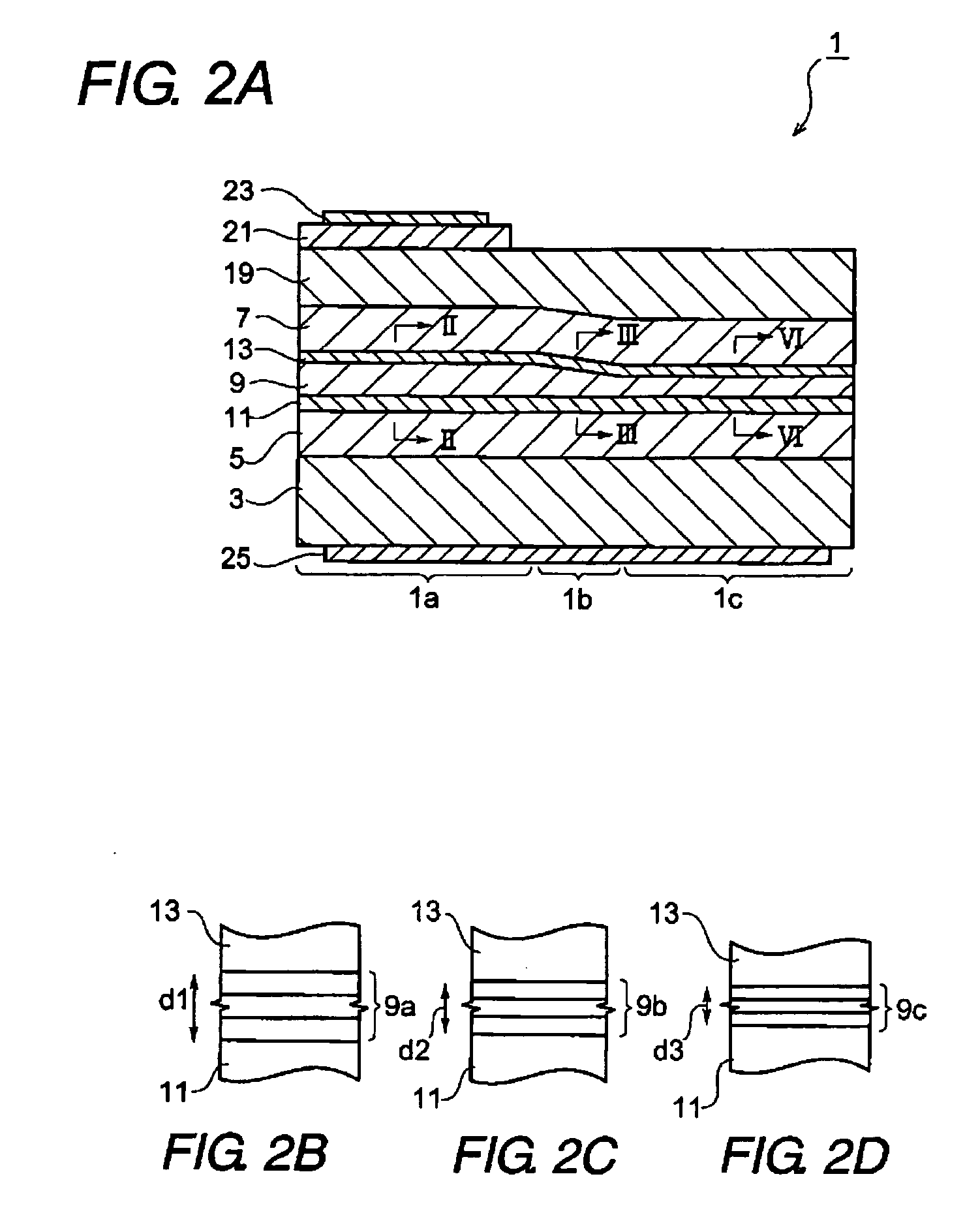
[0031]FIG. 1A is a perspective view showing an optical integrated device 1 according to the present invention, and FIG. 1B is a schematic diagram showing a structure of an active region of the optical integrated device 1. From FIG. 2A is a cross section taken along the line I-I in FIG. 1A, while FIGS. 2B to 2D are cross sections taken along the line II-II, the line III-III, and the line IV-IV in FIG. 2A, respectively.
[0032] The optical integrated device 1 comprises a GaAs substrate 3, a first cladding layer 5, a second cladding layer 7, and an active layer 9. The GaAs substrate whose primary surface 3e is (100) crystallographic surface, with a first conduction type, for instance n-type, and provides first to third regions, 3a to 3c, These first to third regions are arranged along an axis Ax. The first cladding layer 5, showing the first conduction type, is formed in whole regions, 3a to 3c. The second cladding layer 7, showing a second conduction type, for instant p-type, is also f...
second embodiment
[0043] Next, a process, in the first hall, or manufacturing the optical integrated device shown in FIG. 1A will be described as referring to drawings from FIG. 3A to FIG. 3D.
[0044] As shown in FIG. 3A, a plurality of semiconductor layers is grown on the GaAs substrate 41 by using the Organo-Metallic Vapor Phase Epitaxy technique (OMVPE). First, the first cladding layer 43 is grown on the GaAs substrate 41. In FIG. 3A, regions from 41a to 41c, which are arranged along a prescribed line, correspond to regions from 3a to 3c of the GaAs substrate 3 shown in FIG. 1A
[0045] Next, the active layer 47 and two opal confinement layers, 45 and 49, are grown on the first cladding layer 43. Prior to the growth of these layers, a mask 42 is formed on the first cladding layer 43. FIG. 5B is a plan view showing the plane shape of the mask 42. That is, the mask comprises first to third portions, 42a to 42c corresponding to regions from 41a to 41c of the GaAs substrate 41. The widths of respective po...
third embodiment
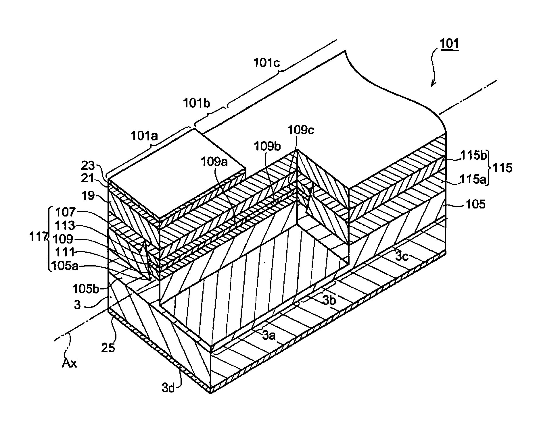
[0063]FIG. 7A is a perspective view showing another optical integrated device 101 according to the third embodiment of the invention, and FIG. 7B is a schematic diagram showing a layer of an active layer of the device shown in FIG. 7A.
[0064] The optical integrated device 101 provides a similar structure to those shown in the previously explained device 1 except that the active layer 109, the first cladding layer 105, and the upper and lower optical confinement layers, 111 and 113, form a mesa 117, while only the upper cladding layer makes the ridge in the first embodiment.
[0065] As explained in the former embodiment, the mesa 117 extends from the first region 3a to the third region 3c. The active layer 109a in the first device 101a also smoothly continues to the third active layer 109c via the second active layer 109b. The active layers, from 109a to 109c, are sandwiched by the first and second optical confinement layers, 111 and 113, in whole regions, 101a to 101c. Therefore, adv...
PUM
 Abstract
Description
Claims
Application Information