
Article comprising an oxide layer on a GaAs-based semiconductor structure and method of forming same

a gaas-based semiconductor and oxide layer technology, applied in the direction of vacuum evaporation coating, polycrystalline material growth, crystal growth process, etc., can solve the problems of significant limited performance, integration level and marketability of both digital and analog gaas-based devices and circuits, and the inability to meet the requirements of many applications of gallium oxides fabricated by this techniqu

Inactive Publication Date: 2005-10-06
NXP USA INC
View PDF2 Cites 9 Cited by
  • Summary
  • Abstract
  • Description
  • Claims
  • Application Information

AI Technical Summary

Benefits of technology

The present invention provides a new and improved method of manufacturing a gate quality Ga2O3-compound semiconductor structure. This method results in a structure with a low defect density related to oxygen vacancies, which is suitable for MOSFET applications. The method involves depositing layers of gallium oxide and a galvanic oxide-galvanic gadolinium oxide mixture on a supporting semiconductor structure, resulting in a high-quality interface and low oxide leakage current density. The invention also provides a compound semiconductor structure that includes a dielectric layer structure formed from a layer of Ga2O3 followed by a layer of Ga—Gd-oxide, which has both a low defect density and a low oxide leakage current density.

Problems solved by technology

Due to a lack of insulating layers having low interface state density and stable device operation on gallium arsenide (GaAs) based semiconductors, the performance, integration level and marketability of both digital and analog GaAs based devices and circuits is significantly limited.
However, the properties of gallium oxides fabricated by this technique are inadequate for many applications because of high oxide bulk trap densities and excessive leakage current.
Consequently, the performance of unipolar and bipolar devices is affected and the fabrication of stable and reliable metal-oxide-semiconductor field effect transistors (MOSFET) based on compound semiconductors has been problematic.
As discussed in U.S. Pat. No. 6,159,834, it has been determined that the aforementioned technique does not produce a high quality Ga2O3 layer because of oxygen vacancies in the layer that give rise to defects that cause unacceptable oxide trap densities.
However, oxide bulk trap densities are still unacceptably high and significant leakage current is observed.
While this oxide layer has an acceptably low leakage current density, Ga2O3(Gd2O3)—GaAs interface state densities are relatively high, resulting in unacceptable device performance.

Method used


Image

  • Article comprising an oxide layer on a GaAs-based semiconductor structure and method of forming same
  • Article comprising an oxide layer on a GaAs-based semiconductor structure and method of forming same

Examples


Embodiment Construction

[0017] The present inventors have surprisingly determined that a high quality, low defect dielectric layer structure can be formed from a gallium-oxide / GaAs interface followed by a Ga—Gd oxide layer. In contrast, prior art dielectric layers have been composed of either a gallium-oxide / GaAs interface or a Ga—Gd oxide / GaAs interface.

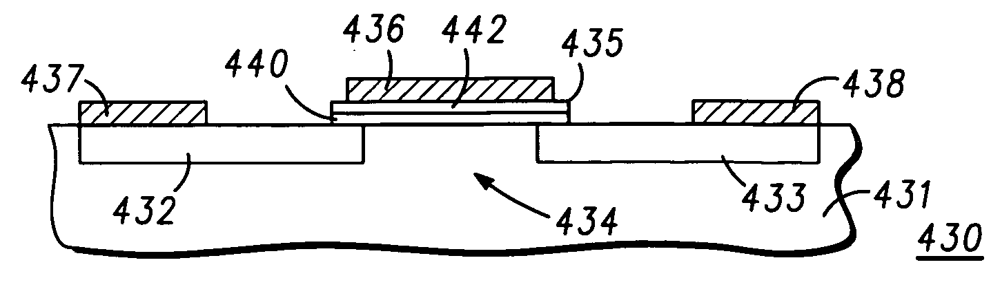
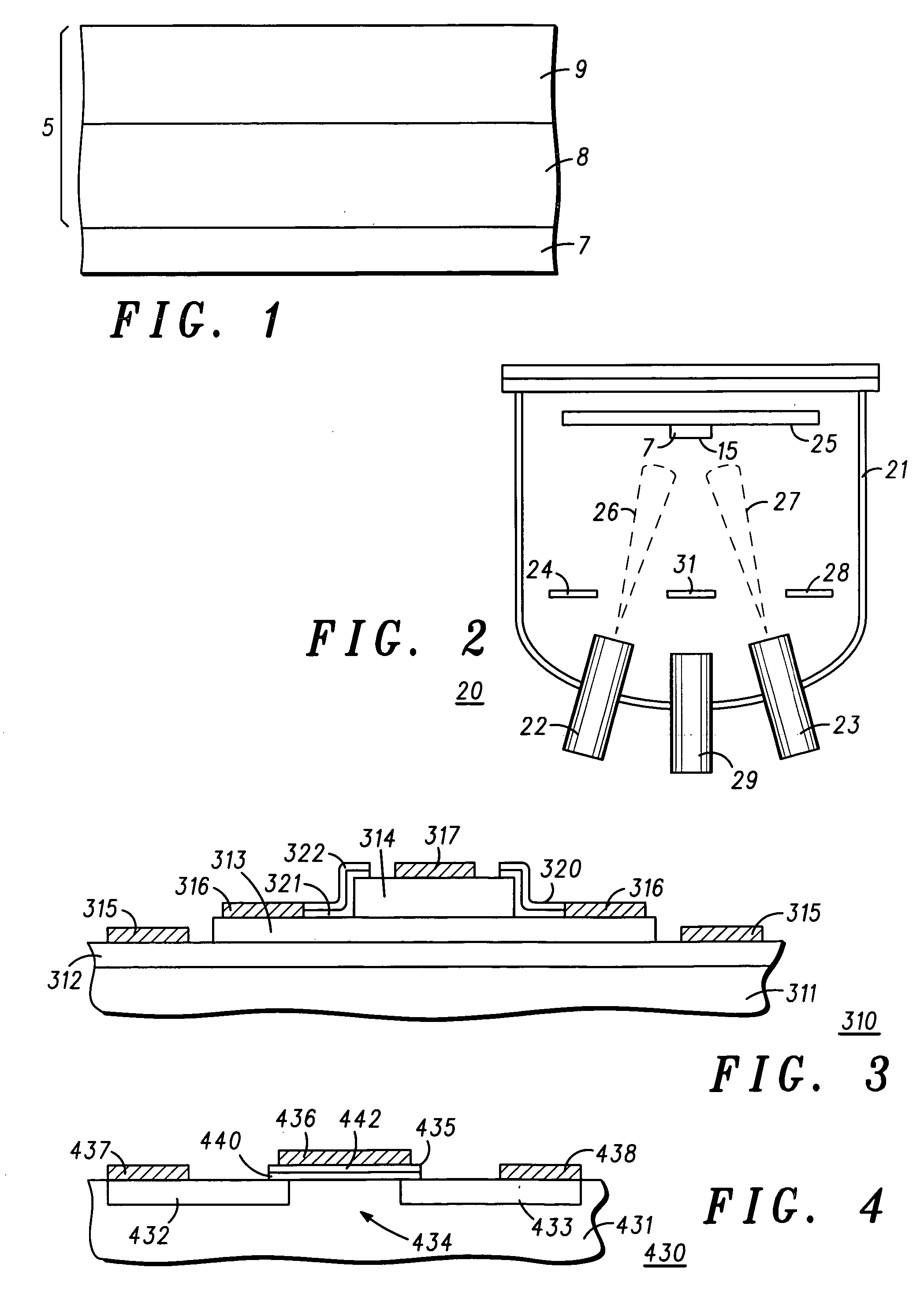
[0018] Referring specifically to FIG. 1 a simplified sectional view of a partial semiconductor structure is illustrated with a dielectric layer structure deposited thereon in accordance with the present invention. The partial semiconductor structure includes a GaAs-based supporting semiconductor structure 7, illustrated for simplicity as a single layer. Basically, structure 7 includes any semiconductor substrate, epilayers, heterostructures or combinations thereof having a surface to be coated with the dielectric layer structure. In general, the substrate is GaAs or a GaAs based material (III-V material) and the epilayers are GaAs based material epitaxial...


PUM

PropertyMeasurementUnit
interface recombination velocitiesaaaaaaaaaa
thicknessaaaaaaaaaa
thicknessaaaaaaaaaa

Abstract

A compound semiconductor structure is provided, which includes a GaAs-based supporting semiconductor structure having a surface on which a dielectric material is to be formed. A first layer of gallium oxide is located on the surface of the supporting semiconductor structure to form an interface therewith. A second layer of a Ga—Gd oxide is disposed on the first layer. The GaAs-based supporting semiconductor structure may be a GaAs-based heterostructure such as an at least partially completed semiconductor device (e.g., a metal-oxide field effect transistor, a heterojunction bipolar transistor, or a semiconductor laser). In this manner a dielectric layer structure is provided which has both a low defect density at the oxide-GaAs interface and a low oxide leakage current density because the dielectric structure is formed from a layer of Ga2O3 followed by a layer of Ga—Gd-oxide. The Ga2O3 layer is used to form a high quality interface with the GaAs-based supporting semiconductor structure while the Ga—Gd-oxide provides a low oxide leakage current density.

Description

FIELD OF THE INVENTION [0001] The present invention relates generally to articles that include dielectric oxide layers formed on a GaAs-based semiconductor structure. BACKGROUND OF THE INVENTION [0002] In the semiconductor art it is often desirable to form dielectric layers or films on various supporting structures, such as the gate insulator in field effect transistors, an insulator or passivation layer covering various areas (e.g. the extrinsic base region) of other types of transistors, such as HBTs and the like, an insulator or passivation layer surrounding the mesa or walls of a vertical cavity surface emitting laser or edge emitting lasers, etc. Regardless of the use, it is generally imperative that the dielectric layer or film be a good insulator with low defect density to enable device operation and enhance / maintain device performance. Also, the thickness of the layer must be sufficient to provide the required characteristics of the semiconductor devices, e.g. leakage curren...

Claims


Application Information

Patent Timeline
Patent Type & Authority Applications(United States)
IPC IPC(8): C23C14/08C30B23/02C30B29/16H01L21/28H01L21/31H01L21/316H01L29/423H01L29/51
CPCC23C14/08C30B23/02C30B29/16H01L21/02112H01L21/02192H01L21/022H01L21/02269H01L21/28194H01L21/28264H01L21/31604H01L21/31666H01L29/4232H01L29/511H01L29/513H01L29/517H01L21/02178H01L21/00H01L21/28H01L29/76
Inventor PASSLACK, MATTHIASMEDENDORP, NICHOLAS WILLIAM JR.
Owner NXP USA INC
Learn More