Chemical treatment of material surfaces

a technology of chemical treatment and material surface, applied in the field of surface treatment, can solve the problems of wide spread of polymer adhesion problems, inability to naturally wettable, hydrophobic surface of cured polymer materials, and poor adhesion of polymer solutions to adjacent cured polymer surfaces, etc., to achieve the effect of reducing the contact angle of the surface, simple and inexpensive, and promoting the wettability of the surfa

Inactive Publication Date: 2005-10-27
POLYSET +1
View PDF13 Cites 52 Cited by
  • Summary
  • Abstract
  • Description
  • Claims
  • Application Information

AI Technical Summary

Benefits of technology

[0009] The present invention meets the aforementioned needs and unexpectedly provides a simple, inexpensive, and practical method for promoting the wettability of polymer surfaces, as well as that of silicon-containing materials. The novel process dramatically decreases the contact angle of the surface, a...

Problems solved by technology

However, polymer adhesion problems are wide-spread throughout industry, largely because many cured polymers in the solid-state have chemically inert and nonporous surfaces with low surface tensions.
The surfaces of these cured polymer materials are hydrophobic and not naturally wettable.
Thus, subsequently deposited polymer solutions adhere poorly to the surface of the adjacent cured polymer.
However, gas plasma pretreatments are expensive to operate on ...

Method used


Image

  • Chemical treatment of material surfaces
  • Chemical treatment of material surfaces
  • Chemical treatment of material surfaces

Examples


example 1

[0038] An N-type, 4-inch silicon wafer having a resistivity of 0-0.02 ohm-cm was used as the substrate. After standard RCA cleaning an adhesion promoter (HMDS) was spin-coated onto the wafer at 3000 rpm for 40 sec. The wafer was then annealed in air at 100° C. for 10 min. A siloxane epoxy prepolymer solution containing structure (IIB), wherein the ratio of p to q was about 2:1, was spin-coated onto the wafer at 3000 rpm for 100 sec to a thickness of 0.5 micron to form a first layer. The first polymeric film / wafer was baked under vacuum of 10−3 torr for 1 hour at 100° C. The film was then cured at 165° C. for 2 hours, followed by a thermal anneal at 250° C. under nitrogen gas flow for 1 hour to cross-link the polymer. The contact angle of the cured first polymer layer was measured to be 70°.

example 2

[0045] The procedure of Example 1 was followed, and a second prepolymer layer was spun onto the surface of the cured first polymer layer (3000 rpm for 100 sec to a thickness of 0.5 micron). The prepolymer deposited as the second layer was the same as that deposited as the first layer polymer described in Example 1. However, the first polymer layer surface dewetted during the spin on process of the second prepolymer layer, as shown in the left side of FIG. 4, described below.

example 3

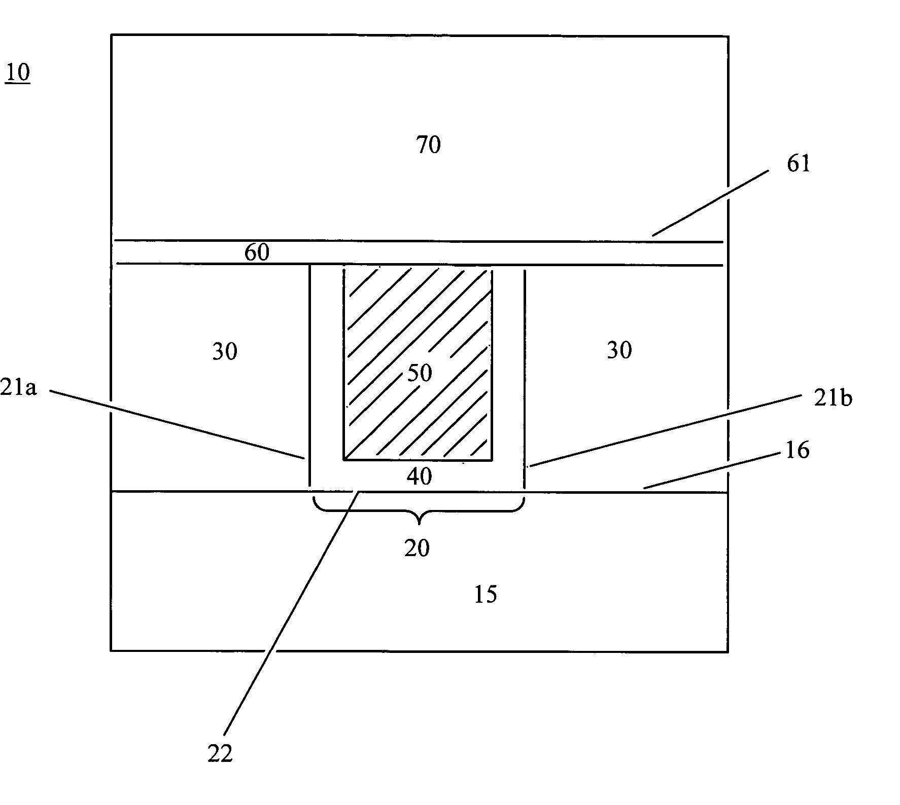
[0051]FIG. 5 is a cross-sectional view of a portion 10 of a semiconductor structure fabricated using conventional damascene processing, wherein trenches (lines) and vias (holes) are etched into interlayer dielectric 30. Initially, a low-k prepolymer, such as parylene, is deposited by chemical vapor deposition (CVD) (and cured) to a thickness typically of up to 0.7 μm onto top surface 16 of semiconductor substrate 15 made of polysilicon, for example, to form first polymeric low-k interlayer dielectric 30. Via 20 is etched into first polymeric low-k interlayer dielectric 30. Ta-based liner 40, made of tantalum, TaN, or TaSiN, is conformally deposited onto sidewalls 21a and 21b and bottom 22 of via 20 (and any trenches, not shown), followed by deposition of copper 50 and planarization. Silicon-containing dielectric cap 60 made of SiN, SiC, SiCH, or SiCN is then deposited by CVD onto the top surfaces of copper line 50, Ta-based barrier 40 and low-k polymeric dielectric 30 to a thickness...


PUM


Abstract

A method for treating the surfaces of materials to improve wettability and adhesion of subsequently deposited polymer layers is disclosed. Suitable materials for practice of the method include polymeric materials and silicon-containing materials is disclosed. The method involves contacting at least a portion of the surface of the material with an aqueous solution of sulfuric acid or phosphoric acid, followed by rinsing with water. After the acid treatment, the contact angle of the surface decreases, and subsequently deposited polymer coatings easily wet the material's surface and exhibit enhanced adhesion. The method may be used to fabricate useful structures, such as semiconductor structures, optical waveguide structures, and coated articles.

Description

CROSS-REFERENCE TO RELATED APPLICATIONS [0001] This Application is related to the following U.S. Patent Applications: U.S. Patent Application entitled “SILOXANE EPOXY POLYMERS FOR LOW-κ DIELECTRIC APPLICATIONS” being filed concurrently herewith under Atty Dkt. No. 0665.020; and U.S. Patent Application entitled “SILOXANE EPOXY POLYMERS AS METAL DIFFUSION BARRIERS TO REDUCE ELECTROMIGRATION” being filed concurrently herewith under Atty Dkt. No. 0665.021. Each of these Applications is hereby incorporated by reference herein in its entirety. FIELD OF THE INVENTION [0002] The present invention relates to treating the surface of a material with a mineral acid, and more particularly to using the acid to improve the wettability and adhesive properties of the material surface. BACKGROUND OF THE INVENTION [0003] Throughout industry, there are many examples of organic polymers being formed adjacent a polymeric material. For instance, in the fabrication of integrated circuits, multiple polymer...

Claims


Application Information

Patent Timeline
IPC IPC(8): G02B6/138H01L21/3105H01L21/312H05K3/36
CPCG02B6/138H01L21/02126H01L21/02216H01L21/02282H01L21/3122H01L21/02307H01L21/31058H01L21/312H01L21/3121H01L21/02304
Inventor WANG, PEI-LLU, TOH-MINGMURARKA, SHYAM P.GHOSHAL, RAMKRISHNA
Owner POLYSET
Why Eureka
Try Eureka