Method of manufacturing semiconductor integrated circuit device having capacitor element

a technology of capacitor element and integrated circuit, which is applied in the direction of semiconductor/solid-state device details, digital storage, instruments, etc., can solve the problems of deteriorating soft error resistance, achieve the effect of improving the soft error resistance of memory cells, improving the degree of sram integration, and increasing the potential fluctuation of storage nodes

Inactive Publication Date: 2005-11-03
ACACIA RES GROUP
View PDF21 Cites 6 Cited by
  • Summary
  • Abstract
  • Description
  • Claims
  • Application Information

AI Technical Summary

Benefits of technology

[0014] An object of the present invention is to provide a technique capable of improving the soft error resistance of an SRAM adopting the bulk CMOS type.
[0056] According to the means described above, one of the electrodes of the capacitor element composed of the second conductive film, the third conductive film and the insulating film interposed between the two conductive films, is connected to one storage node, and the other electrode is connected to the other storage node, so that sufficient charge is fed to the storage nodes through the capacitor element. As a result, even when the memory cell is miniaturized or when the operating voltage is lowered, the potential fluctuation of the storage nodes due to alpha rays is suppressed to improve the soft error resistance of the memory cell.
[0057] By constructing a capacitor element of the peripheral circuit using the two-layered conductive film deposited on the semiconductor substrate, according to the means described above, the area occupied by the elements can be made smaller than that of the capacitor element using a diffused layer (pn junction) formed over the semiconductor substrate, so that the area of the peripheral circuit can be reduced to raise the degree of integration of the SRAM.
[0058] By connecting the semiconductor regions of the MISFETs and the wiring lines through the pad layers which are formed at the same step as that of the electrodes of the capacitor element, according to the means described above, the mask aligning margin at the time when the connection is made over the semiconductor region by etching using a photoresist as the mask can be reduced to reduce the area of the MISFETs and thereby to raise the degree of integration of the SRAM.
[0059] By thinning a portion of the insulating film covering the gate electrodes prior to the step of making contact holes reaching the gate electrodes, according to the means described above, the gate electrodes can be exposed by etching in a short time, so that the remaining regions can be prevented from being over-etched to prevent the erosion of the field dielectric film.

Problems solved by technology

If the operation voltage further drops, the amount of charge stored in the storage node drops, so that the potential fluctuation of the storage node due to alpha rays cannot be suppressed, deteriorating the soft error resistance.

Method used


Image

  • Method of manufacturing semiconductor integrated circuit device having capacitor element
  • Method of manufacturing semiconductor integrated circuit device having capacitor element
  • Method of manufacturing semiconductor integrated circuit device having capacitor element

Examples


embodiment 1

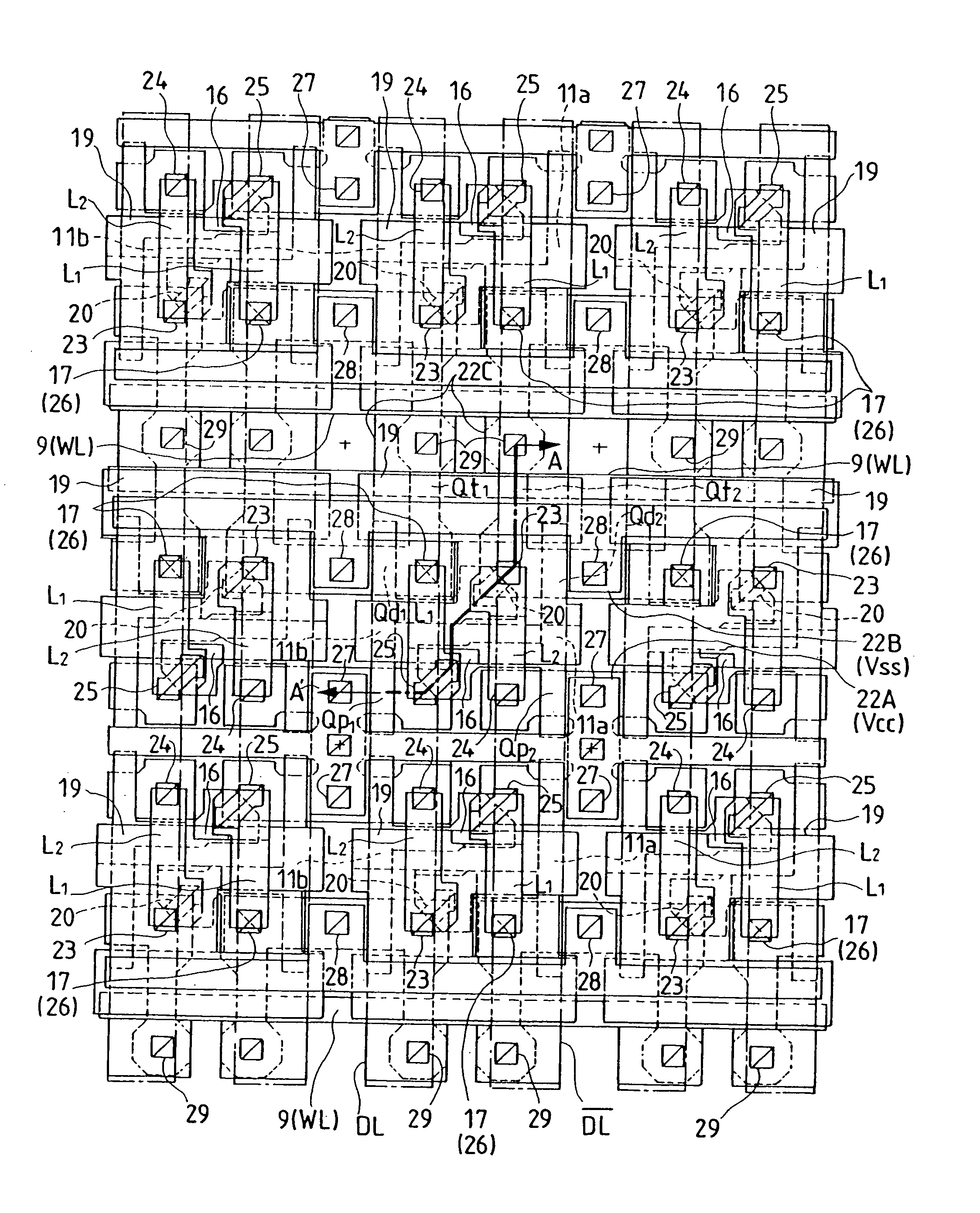
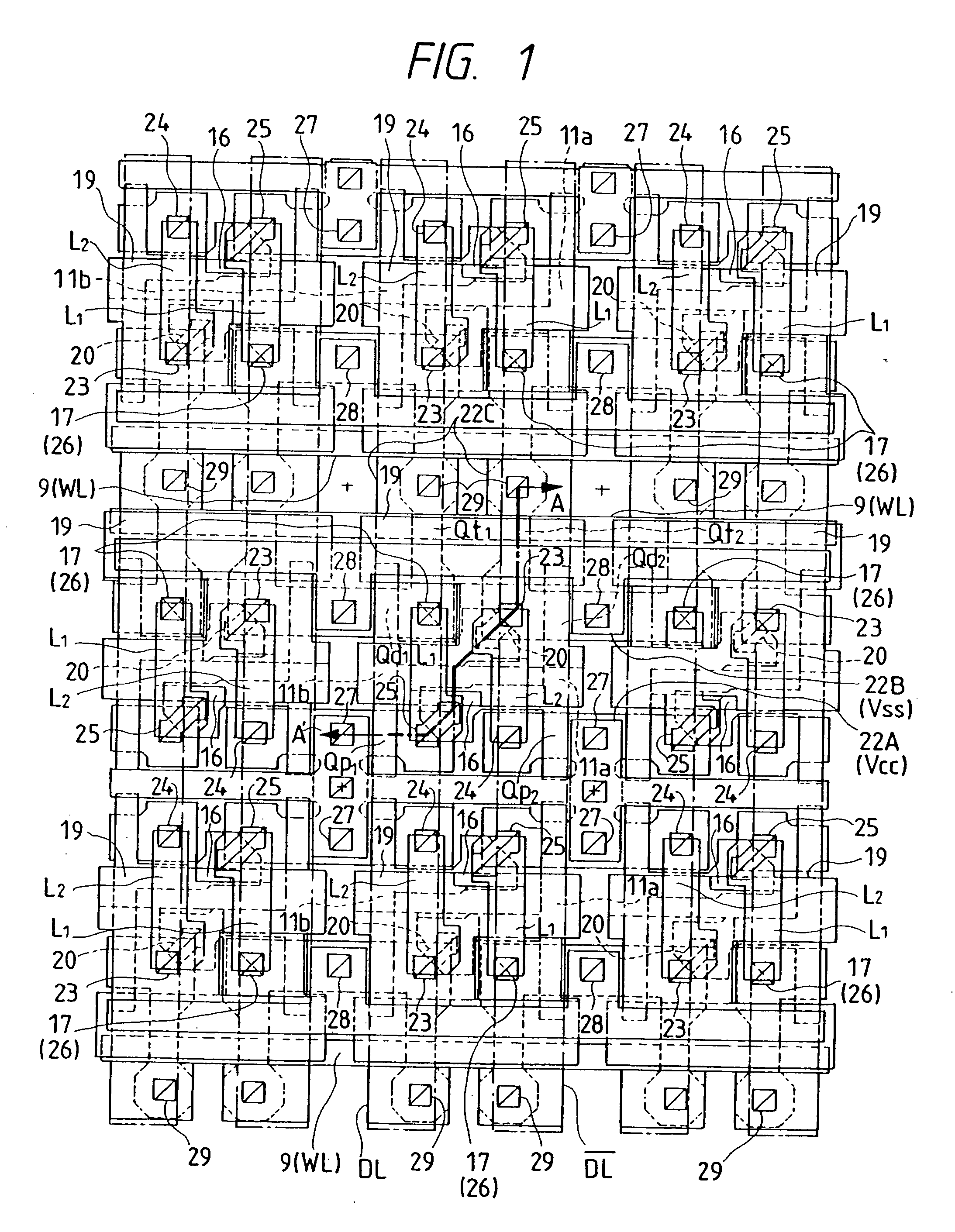
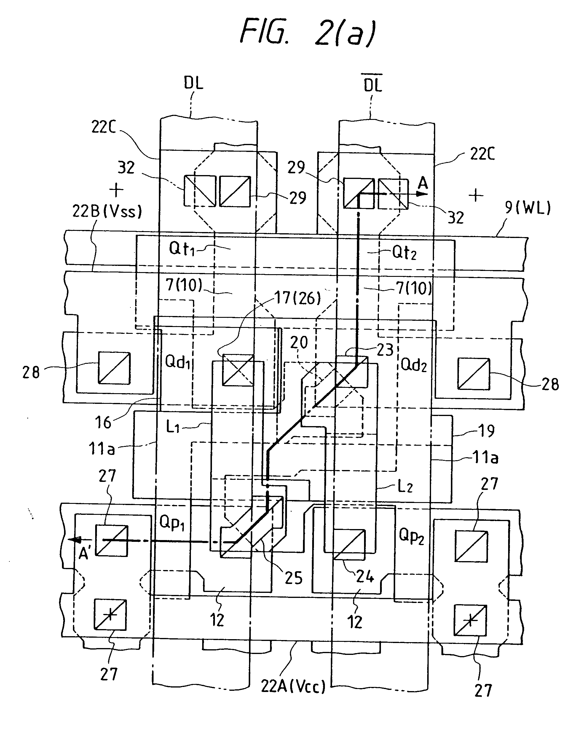
[0127]FIG. 4 is an equivalent circuit diagram of a memory cell of an SRAM of the present embodiment. As shown, this memory cell is constructed of a pair of driver MISFETs Qd1 and Qd2, a pair of load MISFETs Qp1 and Qp2 and a pair of transfer MISFETs Qt1 and Qt2, which are arranged at the intersections of a pair of complementary data lines (i.e., a data line DL and a data line / (bar) DL) and a word line WL. The driver MISFETs Qd1 and Qd2 and the transfer MISFETs Qt1 and Qt2 are of n-channel type, whereas the load MISFETs Qp1 and Qp2 are of p-channel type. In other words, the memory cell is of complete CMOS type using the four n-channel MISFETs and the two p-channel MISFETs.

[0128] Of the six MISFETs constituting the aforementioned memory cell, the paired driver MISFETs Qd1 and Qd2 and the paired load MISFETs Qp1 and Qp2 constitute together a flip-flop circuit serving as an information storage unit for storing information of 1 bit. One (storage node A) of the input / output terminals of ...

embodiment 2

[0169] A process for manufacturing the memory cells of the SRAM of the present embodiment will be described with reference to FIGS. 24 to 38. Incidentally, of the individual Figures showing the memory cell manufacturing process, the top plan views show only the conductive films and the contact holes but not the insulating films.

[0170]

[0171] First of all, as shown in FIG. 24, there are formed on the principal faces of the active regions of the p-type well 3 and the n-type well 4: the gate electrode 9 (the word line WL) of the transfer MISFETs Qt1 ant Qt2; the gate electrode 11a common to the load MISFET Qp1 and the driver MISFET Qd1; and the gate electrode 11b common to the load MISFET Qp2 and the driver MISFET Qd2. The steps up to this are identical to those of the foregoing Embodiment 1.

[0172] Next, in the present embodiment, the silicon oxide film 14 over the gate electrodes 11a and 11b is partially etched and thinned by using a photoresist as the mask. The portions thus tinned ...

embodiment 3

[0207] The process for manufacturing the memory cells of the SRAM of the present embodiment will be described with reference to FIGS. 40 to 52. Incidentally, of the individual Figures showing the memory cell manufacturing process, the top plan views show only the conductive films and the contact holes but not the insulating films.

[0208] First of all, as shown in FIG. 40, the first-level layer n-type polycrystalline silicon film is patterned to form the gate electrodes 9 (the word line WL) of the transfer MISFETs Qt1 and Qt2, the gate electrode 11a common to the load MISFET Qp1 and the driver MISFET Qd1, and the gate electrode 11b common to the load MISFET Qp2 and the driver MISFET Qd2 over the principal faces of the active regions of the p-type well 3 and the n-type well 4. Next, the silicon oxide 14 covering the gate electrodes 11a and 11b of the regions where the contact holes for connections of the local wiring lines set up in the later step are made is etched and thinned.

[0209...


PUM


Abstract

In a complete CMOS SRAM having a memory cell composed of six MISFETs formed over a substrate, a capacitor element having a stack structure is formed of a lower electrode covering the memory cell, an upper electrode, and a capacitor insulating film (dielectric film) interposed between the lower electrode and the upper electrode. One electrode (the lower electrode) of the capacitor element is connected to one storage node of a flip-flop circuit, and the other electrode (the upper electrode) is connected to the other storage node. As a result, the storage node capacitance of the memory cell of the SRAM is increased to improve the soft error resistance.

Description

[0001] This application is a Divisional application of Ser. No. 09 / 434,385, filed Nov. 5, 1999, which is a Continuation application of application Ser. No. 09 / 066,763, filed Apr. 28, 1998, which is a Divisional application of application Ser. No. 08 / 682,243, filed Jul. 17, 1996.FIELD OF THE INVENTION [0002] The present invention relates to a semiconductor integrated circuit device and a technique for manufacturing the same and, more particularly, to a technique which is effective when applied to a semiconductor integrated circuit device having an SRAM (Static Random Access Memory). BACKGROUND OF THE INVENTION [0003] The CMOS SRAM, in which are combined a high resistance load type or complete CMOS (Complementary Metal-Oxide-Semiconductor) type memory cell and a peripheral circuit composed of a complementary MISFET (Metal-Insulator-Semiconductor Field-Effect-Transistor) (CMOSFET), has been used for a cache memory of a computer or workstation of the prior art. [0004] The memory cell of...

Claims


Application Information

Patent Timeline
Patent Type & Authority Applications(United States)
IPC IPC(8): G11C11/412H01L21/8244H01L23/522H01L27/10H01L27/11
CPCG11C11/4125H01L23/5222H01L27/0207H01L27/11H01L27/1104H01L2924/0002H01L27/1112Y10S257/903H01L2924/00H10B10/00H10B10/12H10B10/15
Inventor HASHIMOTO, NAOTAKAHOSHINO, YUTAKAIKEDA, SHUJI
Owner ACACIA RES GROUP
Why Eureka
Try Eureka