Parallel multi-electron beam lithography for IC fabrication with precise X-Y translation

a multi-electron beam and lithography technology, applied in the field of parallel multi-electron beam lithography for ic fabrication with precise x-y translation, can solve the problems of low throughput and high magnetic deflection sensitivity, the density of components may soon reach a physical limit, and the use of these wavelengths may not be practical, so as to alleviate the problems of low throughput and high magnetic deflection sensitivity, the effect of low cost and high precision

Inactive Publication Date: 2005-11-17
GORSKI RICHARD M +2
View PDF22 Cites 47 Cited by
  • Summary
  • Abstract
  • Description
  • Claims
  • Application Information

AI Technical Summary

Benefits of technology

[0018] The purpose of this invention is to provide a low cost, thumbnail-sized electron beam lithography apparatus that alleviates the problems of low throughput and high magnetic deflection sensitivity that prevent current e-beam lithography machines from being used in high volume production. This invention employs a large number of stationary micro column electron guns (MCEG) arranged in an K×L array extending over the length and width of each IC circuit pattern that is to be written on the wafer. Because the footprint of the array is approximately equal to the size of the IC pattern, many such MCEG arrays can fit within the circular area of the silicon wafer. In the invention, one MCEG array will be used to write one IC pattern on the wafer and all the MCEGs will write simultaneously. In conventional electron beam lithography machines, the IC circuit pattern is written by magnetically scanning an electron beam across a stationary silicon wafer. The present invention uses a novel reverse approach wherein the silicon wafer is physically moved by a set of orthogonal, high precision, piezoelectric linear stages disposed under the stationary electron beams. The silicon wafer is mechanically translated in the X and Y directions in a serpentine scan pattern while the individual electron beams are pulsed on and off by precise computer control synchronized with the position of the wafer. The computer control system contains stored IC pattern information that controls the timing of the electron beam pulses in accordance with the X-Y position of the wafer such that any circuit pattern can be written. The maximum travel of the silicon wafer in either the X or Y direction is very small and is approximately equal to the spacing between adjacent electron beams. For example, to write a 16 mm×16 mm circuit pattern with an array of 16×16 beams, the maximum displacement of the wafer need only be 1 mm in both the X and Y directions. Each of the 256 electron beams in the array writes a 1 mm×1 mm sub-field of the IC pattern, where each sub-field can be thought of as an M×N array of pixel elements. One pixel element has a size equal to the smallest feature to be drawn on the wafer. The time required to write one sub-field of the IC pattern is simply the product of the time to mechanically scan one line of the sub-field times the number of lines in t

Problems solved by technology

It is well known in the manufacture of ICs that the density of components may soon reach a physical limit due to the diffraction effects of light.
Diffraction distortion gives rise to a blurring of the shadow of the edge of an object or aperture.
However, the use of these wavelengths may not be practical due to problems arising from the opaqueness of the conventional glass materials making up the optical lenses.
More exotic and costly materials, or the use of totally reflective optics, may be necessary.
However, this approach requires resolving not only the opaqueness problem, but also the additional problems associated with a liquid in contact with the silicon.
These difficulties have become technologically insurmountable as well as cost prohibitive.
The electron optic

Method used


Image

  • Parallel multi-electron beam lithography for IC fabrication with precise X-Y translation
  • Parallel multi-electron beam lithography for IC fabrication with precise X-Y translation
  • Parallel multi-electron beam lithography for IC fabrication with precise X-Y translation

Examples


Embodiment Construction

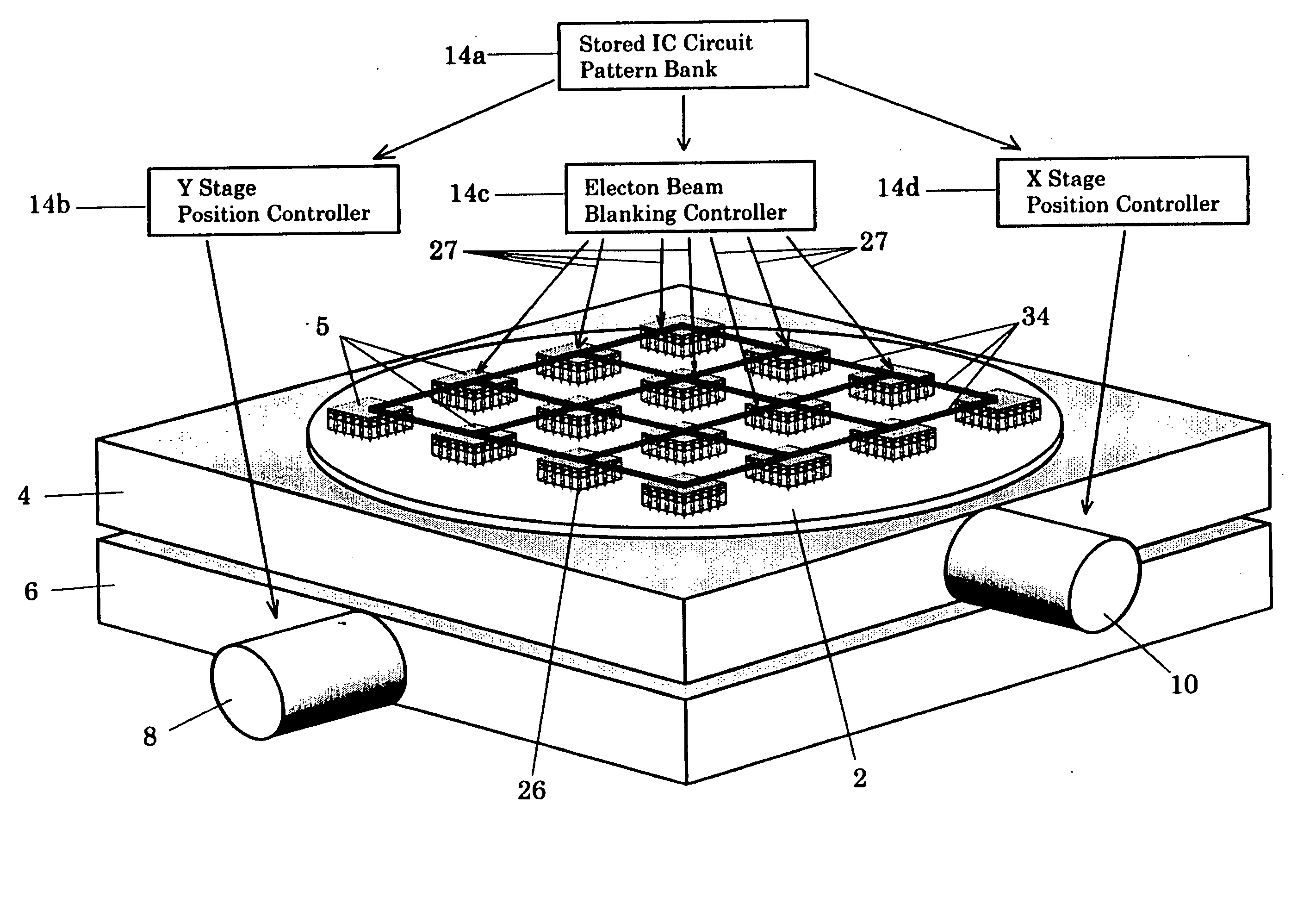
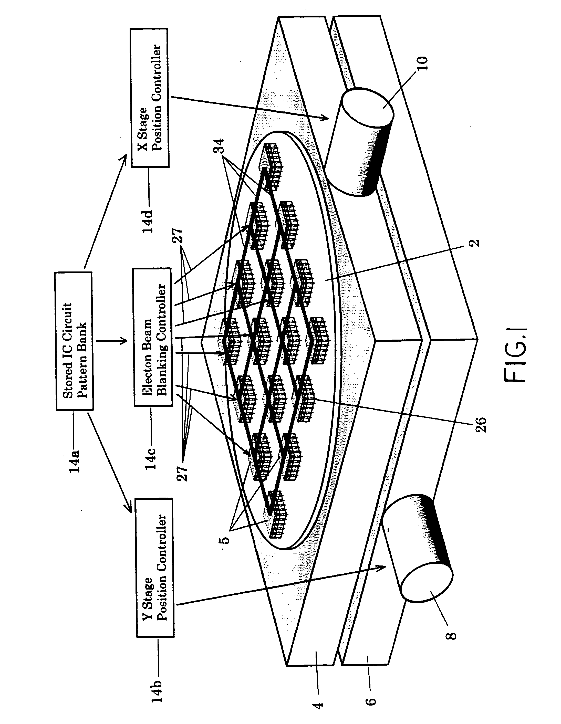
[0026] The following discussion assures that 176, 16 mm×16 mm IC circuit patterns are to be written on a silicon wafer that is 300 mm in diameter using a line width of 65 nm. The concept discussed in the following paragraphs, however, is applicable to any size wafer, IC pattern size and resolution within the scope of the device.

[0027] Referring to FIG. 1, there is shown a conceptual illustration of the 176 MCEG arrays 5 arranged in a rectangular array AIJ across the circular area of a silicon wafer 2 in accordance with a preferred embodiment of the present invention. For reasons of clarity, FIG. 1 does not show all 176 MCEGs as it is a conceptual drawing. The MCEG arrays 5 are spaced every 20 mm in the X and Y directions to allow for about 4 mm of space on each side of an array to accommodate a support frame 34 and electrical connections. Support frame 34 is secured to the framework of the stepper device so that the MCEGs are held in a permanently fixed position with the last elect...


PUM


Abstract

A maskless, direct write electron lithography apparatus for accurately and simultaneously writing plural sub-micron patterns on a silicon substrate employs plural parallel electron beams with precise X-Y mechanical translation of the substrate to provide low cost, high throughput integrated circuit (IC) fabrication. Plural compact micro electron gun assemblies arranged in a I×J rectangular grid each simultaneously expose one IC pattern on the substrate, with each electron gun assembly including a K×L array of individually controlled electron guns emitting K×L electron beams. The regular, small spacing between electron beams in each array, i.e., approximately 1 mm or less, requires a correspondingly small X-Y translation of the substrate to write the entire wafer. Each electron gun array includes plural AC blanked cathodes and DC biased plates having plural aligned beam passing apertures. A computer controlled pattern generator synchronized with wafer X-Y translation controls the duration and timing of the cathode blanking signals.

Description

FIELD OF THE INVENTION [0001] This invention relates generally to the generation and use of high energy, small cross-sectional particle beams and is particularly directed to the use of these types of electron beams arranged in matrix arrays for use in electron beam lithography such as in the fabrication of integrated circuits (ICs) and the chromium masks used in optical lithography. BACKGROUND OF THE INVENTION [0002] The fabrication of ICs is accomplished in large volume production by a process called photolithography. Stated simply, this process uses a monochromatic light source of specified wavelength to expose (harden) a photosensitive material covering a silicon wafer. The monochromatic light shines through a chromium stencil (mask) that contains the circuit pattern to be written on the silicon wafer. The shadow of the circuit pattern passes through a complex optical system designed to de-magnify the image and focus it on the silicon wafer. After a short exposure time of about o...

Claims


Application Information

Patent Timeline
IPC IPC(8): H01J37/04H01J37/302H01J37/317
CPCB82Y10/00B82Y40/00H01J37/045H01J2237/31774H01J2237/0435H01J2237/31766H01J37/3177
Inventor GORSKI, RICHARD M.ROZANSKY, BORISCHEN, HSING-YAO
Owner GORSKI RICHARD M
Why Eureka
Try Eureka