Formation method of electroconductive pattern, and production method of electron-emitting device, electron source, and image display apparatus using this

Inactive Publication Date: 2005-12-01
CANON KK
View PDF1 Cites 9 Cited by
  • Summary
  • Abstract
  • Description
  • Claims
  • Application Information

AI Technical Summary

Benefits of technology

[0006] The present invention aims at providing a production method of an electroconductive pattern which can form an electroconductive pattern effec

Problems solved by technology

Nevertheless, when an electroconductive pattern which has high resistivity regions and low resistance regions is formed in a pattern, the above-mentioned method has such a problem that a facility load is large since there is only way of repeating a step of forming a low r

Method used


Image

  • Formation method of electroconductive pattern, and production method of electron-emitting device, electron source, and image display apparatus using this
  • Formation method of electroconductive pattern, and production method of electron-emitting device, electron source, and image display apparatus using this
  • Formation method of electroconductive pattern, and production method of electron-emitting device, electron source, and image display apparatus using this

Examples


example 1

[0108] As a photosensitive resin, the coating liquid of a methacrylic acid-methyl methacrylate-ethyl acrylate-n-butyl acrylate-azobisisobutyronitrile polymer was applied to a glass substrate (75 mm high×75 mm wide ×2.8 mm thick) with a roll coater on the entire surface, and was dried for 2 minutes at 45° C. on a hot plate. Next, using a negative type photomask, with an extra-high pressure mercury lamp (illuminance: 8.0 mW / cm2) as a light source, the substrate and mask were contacted and were exposed for exposure time of 2 seconds. Next, using deionized water as a chemical developer, the substrate was processed for 30 seconds by dipping, and the resin pattern with film thickness of 1.35 μm was obtained.

[0109] After this resin pattern-formed substrate was soaked for 30 seconds into the deionized water, it was soaked in tris(2,2′-bipyridine)ruthenium(II) chloride aqueous solution (ruthenium content: 1 mass %) for 60 seconds.

[0110] Next, the substrate was pulled out, and was cleaned w...

example 2

[0114] Electrodes were produced similarly to the first example except using a tetraamminepalladium(II) acetate solution (palladium content: 1 mass %) as the metallic compound solution. The sheet resistance value of the metal palladium portion was 30 Ω / sq, and the sheet resistance value of the palladium oxide portion was 4.5 kΩ / sq.

example 3

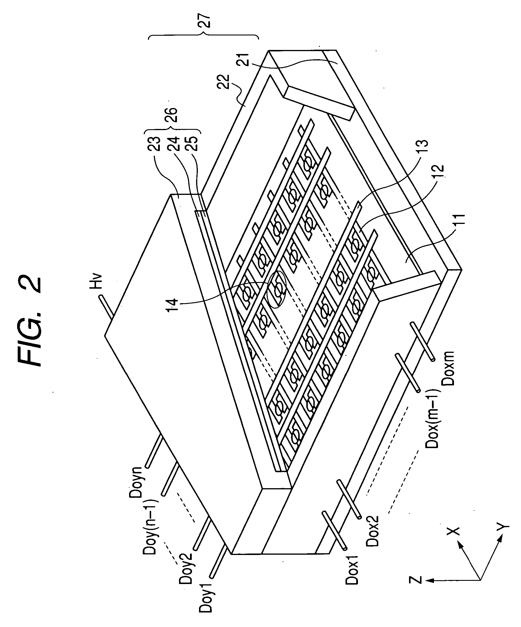
[0115] While producing a plurality of surface conduction type electron-emitting devices using the formation method of an electroconductive pattern of the present invention, wiring for driving the plurality of surface conduction type electron-emitting devices was formed to produce an electron source, and an image display device was further produced using this electron source. Hereafter, production procedure will be described on the basis of FIGS. 2 to 8.

[0116] [Step 1]

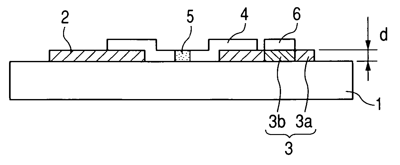
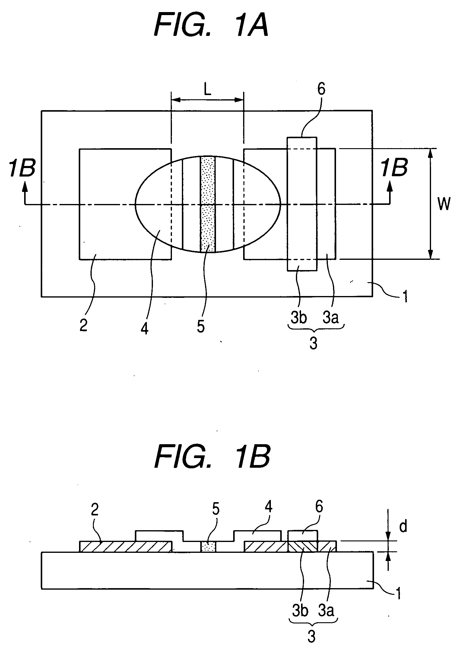
[0117] On the glass substrates 11 with 300 mm wide ×300 mm long ×2.8 mm thick, ruthenium oxide electrodes were formed as the device electrodes 2 and 3 by the same method as the first example (FIG. 3).

[0118] In this example, the device electrode 3 with 60 μm wide and 480 μm long, and the device electrode 2 with 120 μm wide and 200 μm long were made so as to face each other at the inter-electrode gap of 20 μm. In addition, a pitch between the device electrodes 2 and 3 was made 300 μm in a cross direction and 650 μm in l...


PUM


Abstract

In regard to an electroconductive pattern including a high resistivity region partially, by forming a pattern with a photosensitive resin, making the pattern absorb liquid containing a metal component, and baking this, an electroconductive film of metal oxide is formed, this electroconductive film is further covered by a gas shielding layer, and portions which are not shielded are reduced selectively to be made low resistance metal film regions. Since the material which constitutes the electroconductive pattern is hardly removed, a load concerning material reuse is mitigated and material cost is reduced.

Description

BACKGROUND OF THE INVENTION [0001] 1. Field of the Invention [0002] The present invention relates to a method of forming electroconductive patterns such as an electrode and wiring, and a production method of an electron-emitting device, an electron source, and an image apparatus device which form necessary electrodes and wiring using this. [0003] 2. Related Background Art [0004] What are known heretofore as formation methods of electroconductive patterns which become electrodes and wiring are a method of printing an electroconductive paste into a desired pattern by screen printing, and performing drying and baking to form an electroconductive pattern, a transfer method, a method of applying an electroconductive past to an entire surface, and performing drying and baking to form a metal film, and covering a necessary location with a mask such as photoresist and performing etching processing of the other portion to form a necessary electroconductive pattern, and a method of making a m...

Claims


Application Information

Patent Timeline
IPC IPC(8): H01J9/02H01L21/00
CPCH01J1/316H01J9/027H01J2329/0489H01J2201/3165H01J31/127
Inventor FURUSE, TSUYOSHIMORI, SHOSEITERADA, MASAHIRO
Owner CANON KK
Why Eureka
Try Eureka