Field effect transistor and fabrication method thereof

a field effect transistor and fabrication method technology, applied in the direction of transistors, semiconductor devices, electrical equipment, etc., can solve the problems of reducing the cost of conventional fin fet, reducing the length of the channel, increasing the concentration of impurity doping, etc., and reducing the thickness of the gate dielectric. , the difficulty of controlling the short channel effect and the off-state leakage current,

Active Publication Date: 2005-12-22
MICROSOFT TECH LICENSING LLC
View PDF7 Cites 79 Cited by
  • Summary
  • Abstract
  • Description
  • Claims
  • Application Information

AI Technical Summary

Benefits of technology

[0024] An object of the present invention is to provide a new fin FET structure formed on a bulk Si substrate and a fabrication process that overcomes problems and disadvantages of conventional fabrication methods.

Problems solved by technology

However, the following technical problems arise in the scaling.
That is, the scaling (reduction of channel length, reduction of gate dielectric thickness and increase in impurity doping concentration) is accompanied by difficulty in controlling a short channel effect (SCE) and an off-state leakage current of a MOSFET.
The conventional fin FET formed on the SOI has a problem in that, in the view of IC production, the conventional fin FET is costly because the SOI wafer is more expensive than the bulk Si wafer generally used in IC fabrication.
Further, the process of the fin FET formed on the SOI is so complex that a device size can be less freely chosen.
Furthermore, a thicker fin results in a partially depleted device.
This partially depleted device tends to cause such a problem that operation of a transistor becomes destabilized due to floating body effects, in which a body potential of a channel region section floats apart from a fixed potential such as earth and the like.
This SiN layer complicates the fabrication process and the formation of the SiN layer generates, in the fin FET body, mechanical stress that tends to result in a leakage current.
This is a disadvantage of the device.
A fin FET structure described in each of Patent Document 1 and Patent Document 2 has such a problem that a large area is required for each junction section of a source region section and a drain region section.
Thus, the fin FET structure has such a problem that reduction in size cannot be accompanied by reduction of the parasitic capacitance.

Method used


Image

  • Field effect transistor and fabrication method thereof
  • Field effect transistor and fabrication method thereof
  • Field effect transistor and fabrication method thereof

Examples


first embodiment

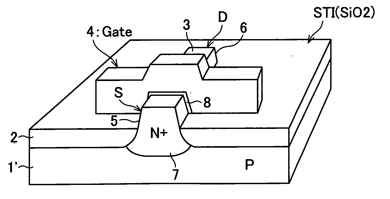
[0045] A fin FET in a first embodiment of the present invention, as illustrated in FIG. 1, is a metal-insulator-semiconductor FET including fin sections 3 and 5 on a semiconductor (ex. silicon) substrate 1. The semiconductor substrate 1 has P-type conductivity. The fin sections 3 and 5 are formed in a fin shape so as to protrude outward from a surface of the semiconductor substrate 1. Any material that can be used for a semiconductor device may be a material of the semiconductor substrate 1. Examples of such a material other than silicon are germanium, silicon-germanium and gallium arsenide. Moreover, the fin has a band shape in a horizontal cross section parallel to the surface of the semiconductor substrate 1 and also has a band shape in a vertical cross section perpendicular to the surface of the semiconductor substrate 1. Each of the band shapes may have constant width from one end to the other end in a longitudinal direction of the fin or may have varied width from one end to t...

second embodiment

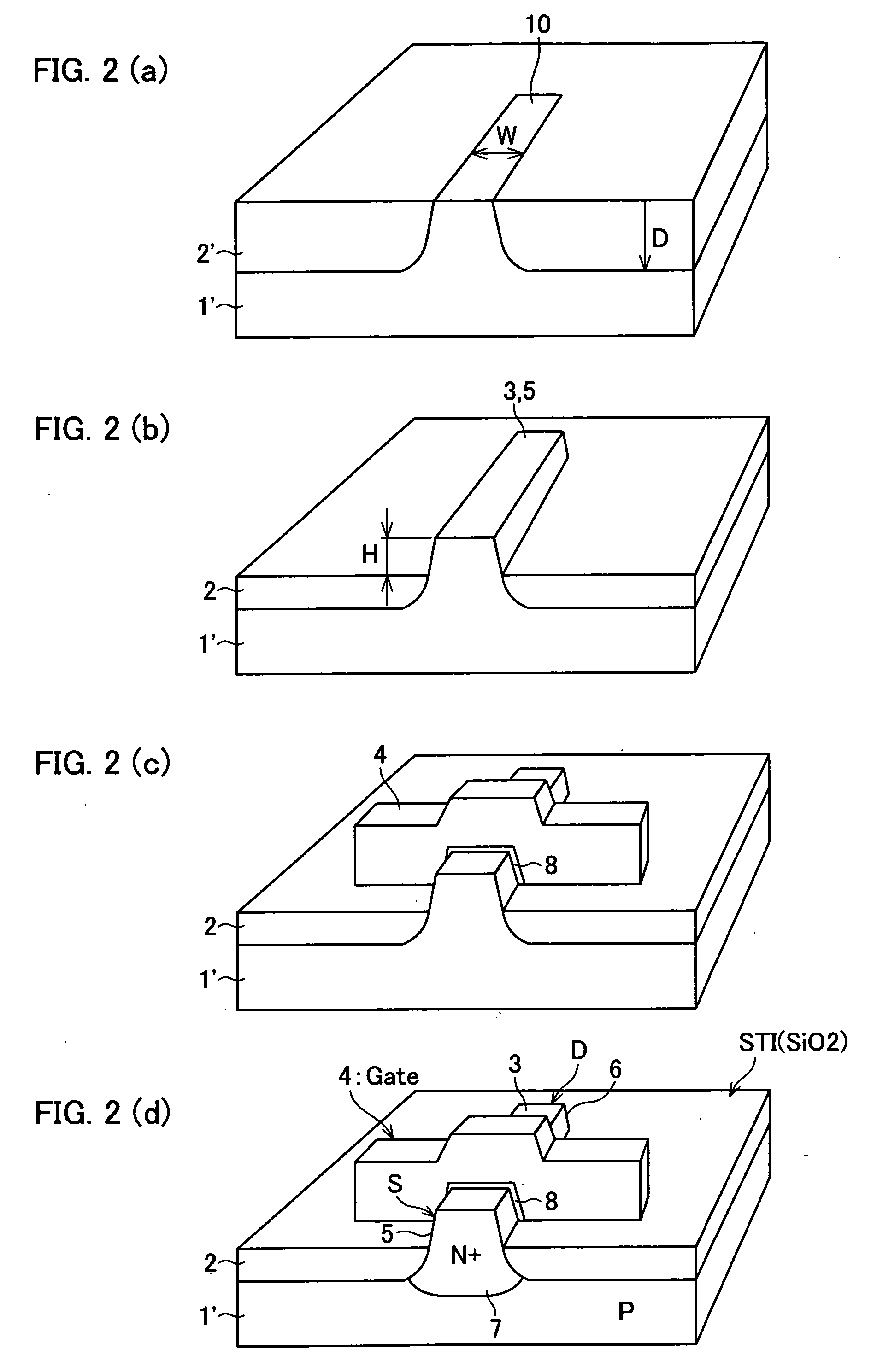
[0065] In a second embodiment of the present invention, as illustrated in FIG. 5, a source region section 5 and a drain region section 3 respectively have an extended source region section 5a and an extended drain region section 3a that are extended in a surface direction of the source region section 5 and the drain region section 3. A fabrication process of an FET of the second embodiment like this, as illustrated in FIG. 6(a) through FIG. 6 (c) and FIG. 7(a) through FIG. 7(c), is explained below. This fabrication process of an FET is performed on a bulk semiconductor wafer substrate 1′. This FET fabrication technique is preferably applicable for formation of a transistor array, such as a gate array, a memory device or the like particularly. Moreover, the bulk semiconductor wafer substrate 1′ is cut, according to need, at a final process so as to serve as the aforementioned semiconductor substrate 1.

[0066] The fabrication process starts with a method identical to the method for fo...


PUM


Abstract

A field effect transistor of the present invention includes, on a semiconductor substrate, (i) a fin section formed in a fin shape protruding from the substrate, (ii) a gate dielectric for covering a channel region section of the fin section, (iii) a gate electrode that is insulated from the channel region section by the gate dielectric and is formed on the channel region section and (iv) an insulating layer for covering a surface of the semiconductor substrate. The fin section is formed so as to extend from the semiconductor substrate through the insulating layer and protrudes outward from a surface of the insulating layer. In this way, the channel region of the fin section is physically in contact with the substrate.

Description

[0001] This Nonprovisional application claims priority under 35 U.S.C. § 119(a) on Patent Application No. 184182 / 2004 filed in Japan on Jun. 22, 2004, the entire contents of which are hereby incorporated by reference. FIELD OF THE INVENTION [0002] The present invention relates to a process and a fabrication method of a semiconductor device. The present invention, specifically, relates to a fin Field Effect Transistor (FET) formed on a bulk Si wafer and a fabrication method thereof. The fin FET formed on the bulk Si wafer is applicable for realization of a highly integrated circuit. BACKGROUND OF THE INVENTION [0003] An integrated circuit tends to be more highly integrated. Accordingly, a scaling technique for a CMOSFET (Complementary Metal Oxide Semiconductor FET) used for the integrated circuit is widely known. The scaling is an industrial method for size reduction and performance improvement. [0004] However, the following technical problems arise in the scaling. That is, the scali...

Claims


Application Information

Patent Timeline
Patent Type & Authority Applications(United States)
IPC IPC(8): H01L21/336H01L29/786
CPCH01L29/7851H01L29/66795
Inventor ADAN, ALBERTO O
Owner MICROSOFT TECH LICENSING LLC
Why Eureka
Try Eureka