Method and apparatus for reducing aspect ratio dependent etching in time division multiplexed etch processes

a technology of multiplexing etching and aspect ratio, which is applied in the direction of fluid pressure measurement, semiconductor/solid-state device testing/measurement, instruments, etc., can solve the problems of incompatibility with device design requirements, difficulty in arde effect, and etching rate drop over time, so as to reduce arde and reduce aspect ratio dependent etching

Active Publication Date: 2005-12-29
PLASMA THERM
View PDF30 Cites 51 Cited by
  • Summary
  • Abstract
  • Description
  • Claims
  • Application Information

AI Technical Summary

Benefits of technology

[0030] Still yet another feature of the present invention is to provide an apparatus for reducing aspect ratio dependent etching during plasma etching of a substrate. The substrate can be a semiconductor substrate such as Silicon, Gallium Arsenide or any known semiconductor, including compound semiconductors e.g., Group II and Group VI compounds and Group III and Group V compounds. The substrate may also be a conductor or a dielectric material such as glass or quartz. The apparatus comprising a vacuum chamber having at least one gas supply source for supplying at least one process gas into the vacuum chamber and an exhaust in communication with the vacuum chamber. The process gas is selected based on the associated process, i.e., deposition of a polymer (octofluorocyclobutane), removal of the polymer (mixture of sulfur hexafluoride, argon and oxygen), or etching of a material (sulfur hexafluoride) from the substrate. The material etched from the substrate is usually silicon. A lower electrode is positioned within the vacuum chamber for applying a bias to the substrate that is placed upon a substrate holder that is connected to the lower electrode. The bias can be powered by RF or DC power. A plasma source generates a plasma within the vacuum chamber. The plasma that is generated is controlled through a process controller for alternately depositing a passivation layer on the substrate by means of a first plasma, removing at least a portion of the deposited passivation layer by means of a second plasma, and etching a material from the substrate by means of a third plasma. A differential interferometer is coupled to the process controller. The differential interferometer generates a laser light beam onto the substrate and measures the difference in depth between at least two different size features on the substrate in real time so that the process can be adjusted through the process controller coupled to the differential interferometer. The process controller varies at least one process parameter in response to the signal generated by the differential interferometer, thereby, reducing ARDE during a TDM process.

Problems solved by technology

First, as an etch process proceeds for a feature of constant width, the feature aspect ratio increases with increasing etch time resulting in an etch rate decrease over time.
The ARDE effect presents challenging complications to MEMS device fabrication.
When structures with various lateral dimensions coexist and are etched at once, the resulting vertical dimensions are different, which may be incompatible with device design requirements.
Even for a single structure, as etching progresses, the vertical etch rate is not constant, which could represent a process control issue.
However, two disadvantages emerge when SOI or SOG wafers are used.
The first disadvantage is notching at the silicon / oxide interface which is often undesirable.
The second disadvantage is SOI and SOG wafers are more expensive than silicon wafers.
While Doh et al. teach in great detail the effects of plasma parameters on RIE lag, their technique uses a single step process and does not teach or suggest its use in a TDM process.
However, the etching process with Cl2 plasma is not a TDM process, and the much slower etch rate and low mask selectivity with Cl2 plasma makes it impractical to etch three-dimensional structures with depths greater than a few tens of micrometers.
In addition, Chung et al. do not teach or suggest the use of real time feedback on the etch depth difference to correct ARDE during the process.
During their experiments they found ARDE was minimized through shorter etch times, low pressures, low platen (RF bias) powers, and increased deposition times. Rickard et al. do not disclose a method to measure the extent of lag in the process in real time.
Furthermore, Rickard et al. do not disclose the use of closed loop adaptive recipe control to minimize ARDE during the TDM process.
Lill et al. teach light reflection from the surface for monitoring the etch rate, but do not teach direct measurement of at least two different feature widths for real time etch depth control.
Furthermore, Lill et al. do not contemplate applying real time control to a time division multiplex process.
As a result Lill et al. do not teach the reduction of etch step time, increased polymer deposition time, reduced polymer removal rate or increased polymer deposition rate as solutions to ARDE in TDM silicon etch processes.
This effect is undesirable.
Laermer et al. do not teach the use of a twin beam interferometer for real-time process feedback.
In addition, Laermer et al. do not teach the use of real time measurement of two features simultaneously to reduce ARDE.

Method used


Image

  • Method and apparatus for reducing aspect ratio dependent etching in time division multiplexed etch processes
  • Method and apparatus for reducing aspect ratio dependent etching in time division multiplexed etch processes
  • Method and apparatus for reducing aspect ratio dependent etching in time division multiplexed etch processes

Examples


Embodiment Construction

[0055] We disclose an improved method and apparatus for reducing, or eliminating, RIE lag (ARDE) in TDM etch processes by adjusting the polymer deposition, the removal of the polymer and / or the etching of the material from the substrate.

[0056] We also disclose the use of a real time metrology device, differential interferometer, for generating a signal indicative of a difference in depth between at least two different size features to reduce, or eliminate, RIE lag (ARDE) in TDM etch processes.

RIE Lag Reduction Examples

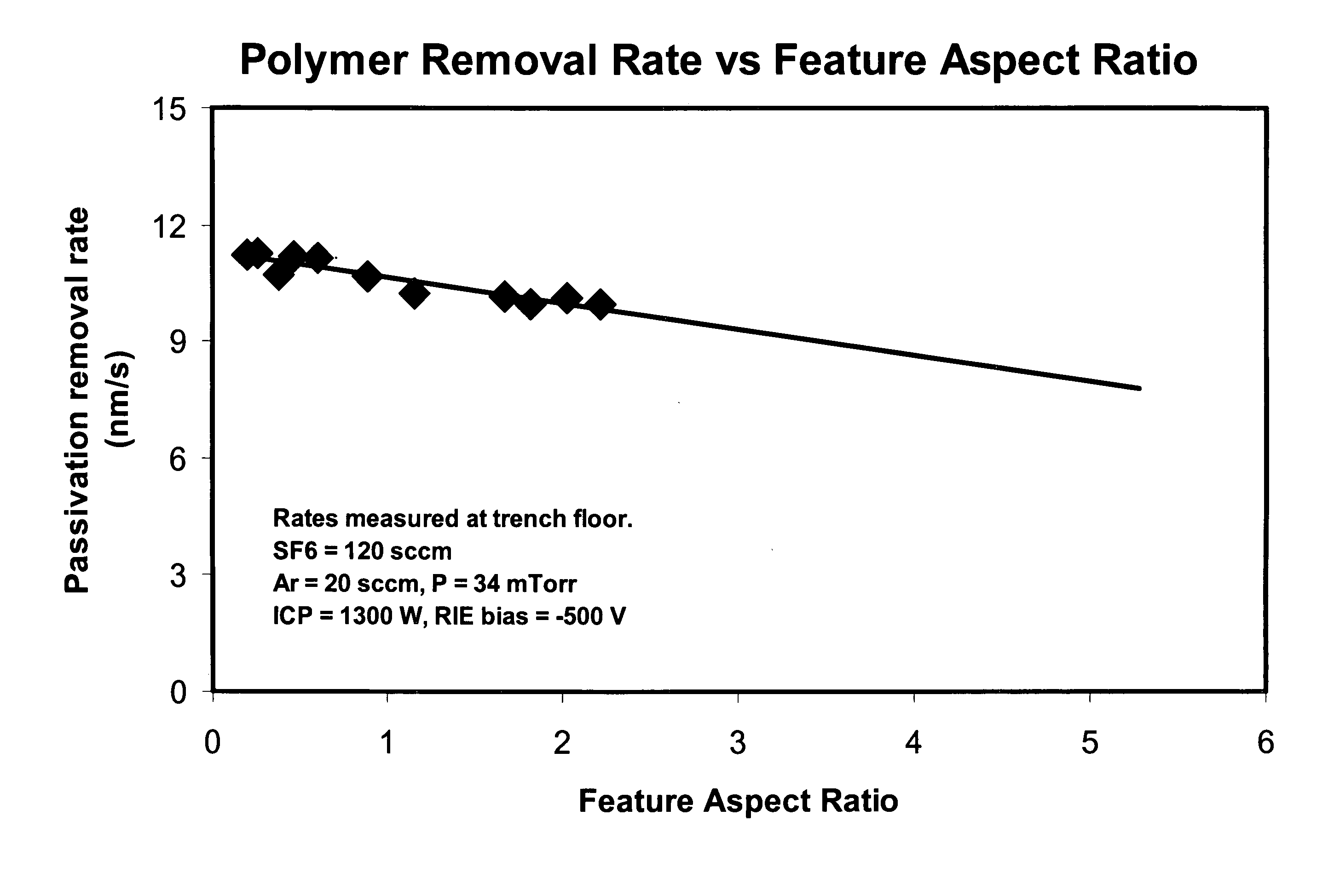
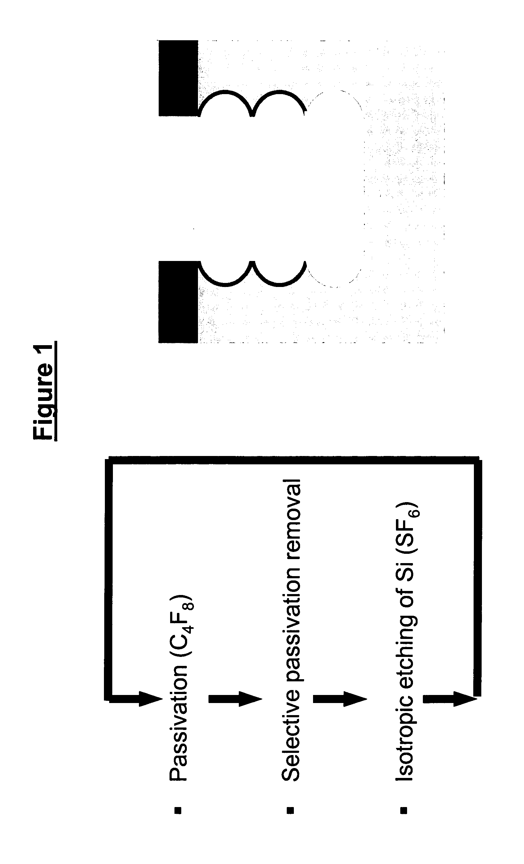
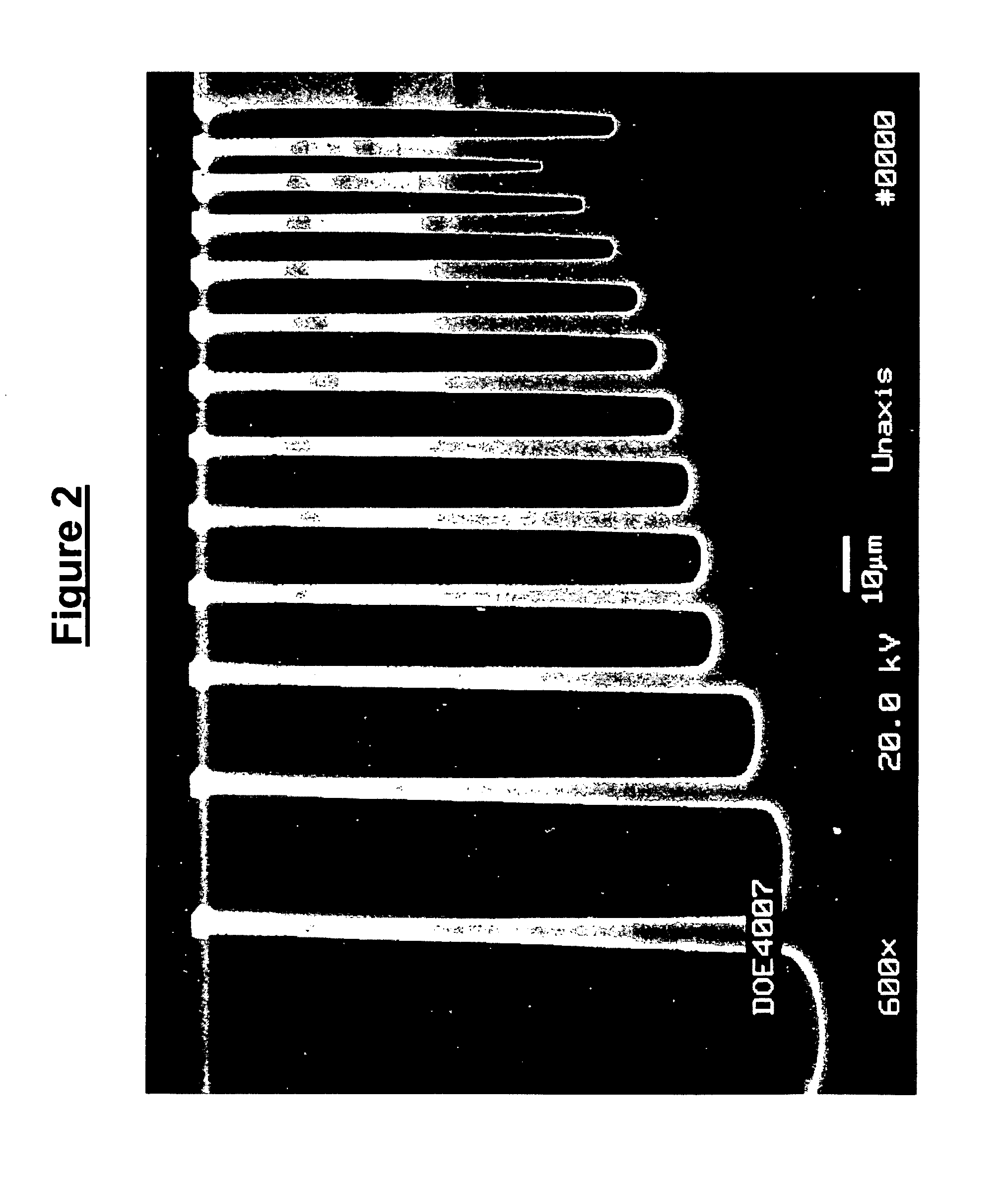
[0057] As made apparent in FIG. 1, one needs to start with the three fundamental physical processes (polymer deposition, polymer removal and isotropic silicon etching) in order to reduce or eliminate RIE lag. The etch and deposition characteristics of all three sub-processes are feature size (aspect ratio) dependent. The feature size dependency however is different for each of the three sub-processes.

[0058] In a typical TDM silicon etch process, the polymer deposi...


PUM

PropertyMeasurementUnit
sizeaaaaaaaaaa
widthsaaaaaaaaaa
depthaaaaaaaaaa

Abstract

The present invention provides a method and an apparatus for reducing aspect ratio dependent etching that is observed when plasma etching deep trenches in a semiconductor substrate through an alternating deposition/etch process. A plurality of different sized features on the substrate are monitored in real time during the alternating deposition/etch process. Then, based on the information received from the monitor, at least one process parameter is adjusted in the alternating deposition/etch process to achieve equivalent etch depths of at least two different sized features on the substrate.

Description

CROSS REFERENCES TO RELATED APPLICATIONS [0001] This application claims priority from and is related to commonly owned U.S. Provisional Patent Application Ser. No. 60 / 584,470 filed Jun. 29, 2004, entitled: A Method and Apparatus for Reducing Aspect Ratio Dependent Etching in Time Division Multiplexed Etch Processes, this Provisional Patent Application incorporated by reference herein.FIELD OF THE INVENTION [0002] This invention relates to a method and apparatus for plasma etching a feature in a substrate. More particularly, the present invention relates to the reduction of aspect ratio dependent etching in the manufacture of high aspect ratio silicon structures by controlling the alternating deposition and etching steps used to etch these structures. BACKGROUND OF THE INVENTION [0003] The fabrication of three-dimensional structures in silicon is used extensively in the manufacture of micro-electro-mechanical (MEMS) devices. Often such structures have high aspect ratios (AR) and dept...

Claims


Application Information

Patent Timeline
Patent Type & Authority Applications(United States)
IPC IPC(8): C23F1/00G01L21/30G01R31/00H01L21/302H01L21/306H01L21/3065H01L21/461H01L21/66
CPCH01L21/30655H01L22/20H01L21/67253
Inventor LAI, SHOULIANGJOHNSON, DAVIDWESTERMAN, RUSSELL
Owner PLASMA THERM
Why Eureka
Try Eureka