

Non-volatile memory and manufacturing method thereof
a manufacturing method and non-volatile technology, applied in the direction of semiconductor devices, transistors, electrical devices, etc., can solve the problems of low threshold voltage value of select transistors, slow memory operation speed, and drop in overall device performance of devices, so as to increase the threshold voltage of select transistors and lower the electrical resistance of select gates
- Summary
- Abstract
- Description
- Claims
- Application Information
AI Technical Summary
Benefits of technology
Problems solved by technology
Method used
Image

Examples
Embodiment Construction
[0023] Reference will now be made in detail to the present preferred embodiments of the invention, examples of which are illustrated in the accompanying drawings. Wherever possible, the same reference numbers are used in the drawings and the description to refer to the same or like parts.
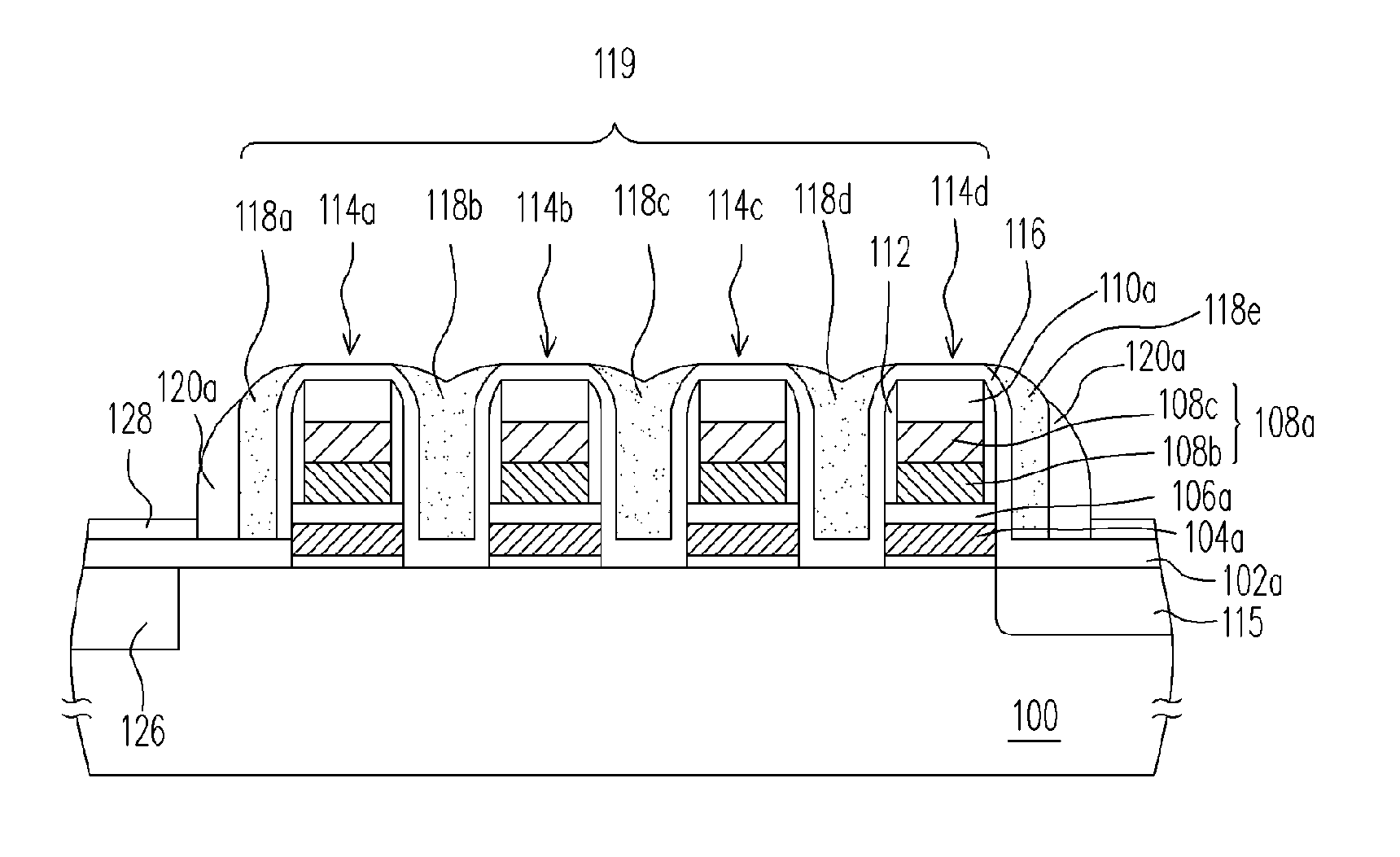
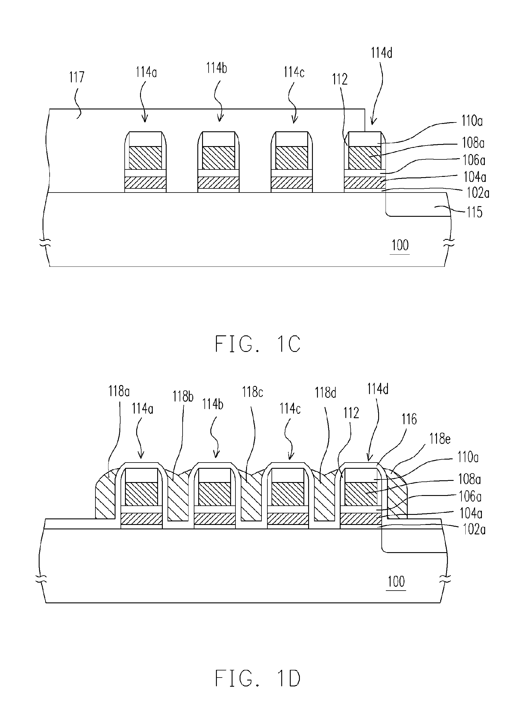
[0024] First, a method of manufacturing a non-volatile memory is provided. FIGS. 1A through 11 are schematic cross-sectional views showing the steps for fabricating a non-volatile memory according to one preferred embodiment of the present invention. The cross-sectional views shown in FIGS. 1A through 11 show only the changes in the active region.
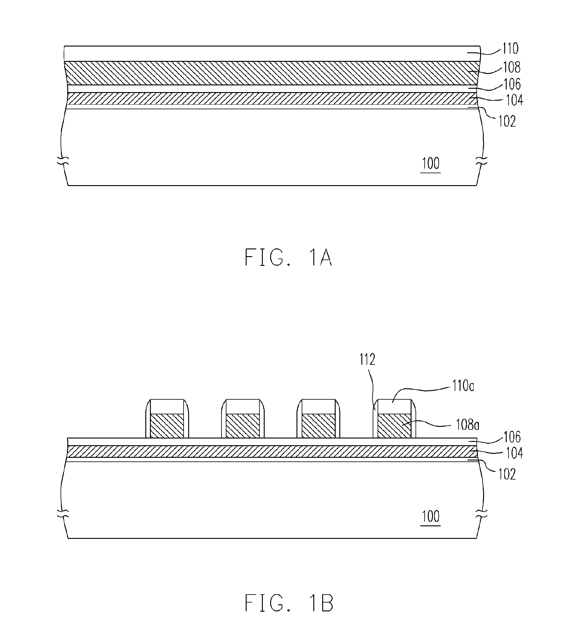
[0025] As shown in FIG. 1A, a substrate 100 such as a silicon substrate is provided. Thereafter, a dielectric layer 102 is formed over the substrate 100. The dielectric layer 102 is, for example, a silicon oxide layer formed in a thermal oxidation process.
[0026] Thereafter, a conductive layer 104 is formed over the dielectric layer 102. The conductive la...
PUM
 Abstract
Description
Claims
Application Information