
Chemical vapor deposition material and chemical vapor deposition

a technology of chemical vapor and material, applied in the field of chemical vapor deposition material and chemical vapor deposition, can solve the problems of reducing the conductivity of the memory cell, affecting the quality of ruthenium, and affecting the quality of ruthenium, and achieve the effect of high-quality ruthenium

Active Publication Date: 2006-02-02
JSR CORPORATIOON
View PDF6 Cites 13 Cited by
  • Summary
  • Abstract
  • Description
  • Claims
  • Application Information

AI Technical Summary

Benefits of technology

[0011] It is an object of the present invention which has been made in view of the above problem to provide a chemical vapor deposition material which can provide a high-quality ruthenium film even when it is very thin and a simple method of forming a ruthenium film from the chemical vapor deposition material.

Problems solved by technology

It is becoming difficult to ensure the capacity of a memory cell with the prior art to meet drastic demand for higher integration and a finer pattern rule for semiconductor devices typified by DRAM (Dynamic Random Access Memory).
However, an oxygen atom contained in this Low-k material is taken into the copper wiring easily to reduce its conductivity.
However, even when these high-dielectric materials are used as a capacitor insulator, a low dielectric layer may be formed at the interface between an electrode and a dielectric, thereby forming an obstacle to the improvement of capacitance.
However, in general, a metal film formed by chemical vapor deposition has poor surface morphology as the assembly state of the fine crystals of the film is sparse.
When this metal film is used as a capacitor electrode, an increase in leak current caused by the concentration of a field occurs.
When a very thin electrode is to be formed so as to realize a fine pattern rule, a film having a defect that metal portions are scattered like islands and not a uniform film is obtained with the result of reduced electric conductivity.
When this film is used as a capacitor electrode, a large capacitor area cannot be obtained and capacitance required for the operation of the capacitor cannot be ensured.
However, in the method making use of these chemical vapor deposition materials, morphology and the step coverage of a 3-D substrate are improved but the obtained film is inferior to a ruthenium film formed by sputtering in conductivity and the formed ruthenium film contains impurities in large quantities.
Therefore, when a ruthenium film formed from any one of these raw materials by chemical vapor deposition is used as an electrode for DRAM, the performance of the DRAM becomes unsatisfactory.
Further, technology making use of these chemical vapor deposition materials has a problem that it is difficult to form a super thin film required for the reduction of the pattern rule (particularly, 10 nm or less) and therefore cannot realize a DRAM having a fine pattern.
However, this method has a problem with production yield due to its complicated process.

Method used


Image

  • Chemical vapor deposition material and chemical vapor deposition
  • Chemical vapor deposition material and chemical vapor deposition
  • Chemical vapor deposition material and chemical vapor deposition

Examples


synthetic example 1

[0043] 5.7 g of N,N′-diisopropylacetamidine was weighed and placed in a 200 ml flask whose inside had been substituted by nitrogen and left at 50° C. under reduced pressure for 60 minutes. After the inside temperature of the flask was returned to room temperature, the flask was filled with dry nitrogen. 50 ml of well dried diethyl ether was added to the flask in a nitrogen atmosphere and stirred to dissolve the above N,N′-diisopropylacetamidine. This solution was cooled to −60° C., and 22 ml of a diethyl ether solution of butyl lithium (concentration of 2.0 mol / l) was added dropwise under agitation over 30 minutes and further stirred for another 3 hours. Agitation was stopped, the inside temperature of the flask was returned to room temperature over 2 hours, and the supernatant was collected with a syringe to obtain a diethyl ether solution of a lithium salt of N,N′-diisopropylacetamidine.

[0044] Meanwhile, 2.1 g of anhydrous ruthenium trichloride was weighed and placed in a 200 ml ...

synthetic example 2

[0046] 2.1 g of N,N′-diisopropylacetamidine was weighed and placed in a 100 ml flask whose inside had been substituted by nitrogen and left at 50° C. under reduced pressure for 60 minutes. After the inside temperature of the flask was returned to room temperature, the flask was filled with dry nitrogen. 20 ml of well dried diethyl ether was added to the flask in a nitrogen atmosphere and stirred to dissolve the above N,N′-diisopropylacetamidine. This solution was cooled to −60° C., and 9 ml of a diethyl ether solution of butyl lithium (concentration of 2.0 mol / l) was added dropwise under agitation over 30 minutes and further stirred for another 3 hours. Agitation was stopped, the inside temperature of the flask was returned to room temperature over 2 hours, and the supernatant was collected with a syringe to obtain a diethyl ether solution of a lithium salt of N,N′-diisopropylacetamidine.

[0047] Meanwhile, 2.1 g of anhydrous ruthenium trichloride was weighed and placed in a 200 ml f...

synthetic example 3

[0049] 6.8 g of N,N′-di-t-butylacetamidine was weighed and placed in a 200 ml flask whose inside had been substituted by nitrogen and left at 50° C. under reduced pressure for 60 minutes. After the inside temperature of the flask was returned to room temperature, the flask was filled with dry nitrogen. 50 ml of well dried diethyl ether was added to the flask in a nitrogen atmosphere and stirred to dissolve the above N,N′-di-t-butylacetamidine. This solution was cooled to −60° C., 22 ml of a diethyl ether solution of butyl lithium (concentration of 2.0 mol / l) was added dropwise under agitation over 30 minutes and further stirred for another 3 hours. Agitation was stopped, the inside temperature of the flask was returned to room temperature over 2 hours, and the supernatant was collected with a syringe to obtain a diethyl ether solution of a lithium salt of N,N′-di-t-butylacetamidine.

[0050] Meanwhile, 2.1 g of anhydrous ruthenium trichloride was weighed and placed in a 200 ml flask w...


PUM


Abstract

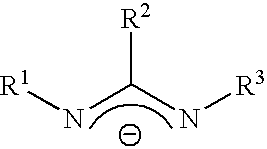
A chemical vapor deposition material comprising a ruthenium compound having a ligand represented by the following formula: wherein R1, R2 and R3 are each independently a hydrogen atom, fluorine atom, trifluoromethyl group or hydrocarbon group having 1 to 10 carbon atoms, and a method of forming a ruthenium film from the chemical vapor deposition material by chemical vapor deposition. A high-quality ruthenium film even when it is very thin can be obtained.

Description

FIELD OF THE INVENTION [0001] The present invention relates to a chemical vapor deposition material and chemical vapor deposition. DESCRIPTION OF THE PRIOR ART [0002] It is becoming difficult to ensure the capacity of a memory cell with the prior art to meet drastic demand for higher integration and a finer pattern rule for semiconductor devices typified by DRAM (Dynamic Random Access Memory). To cope with this, the alteration of the materials of metal films and metal oxide films constituting these devices is becoming necessary to obtain a finer pattern rule. [0003] Particularly, the improvement of a conductive metal film for use in the multi-layer wiring of a semiconductor device is desired. Although aluminum has been used as a wiring material, it is being replaced by copper having a resistivity 60% lower than that of aluminum. In order to improve the conductivity of this copper wiring, a low-dielectric material (Low-k material) is used as an interlayer dielectric material for this...

Claims


Application Information

Patent Timeline
IPC IPC(8): C07F15/00C23C16/00
CPCC23C16/18C07F15/0053C23C14/34H01L21/02365
Inventor SAKAI, TATSUYAHASHIMOTO, SACHIKOMATSUKI, YASUO
Owner JSR CORPORATIOON
Learn More