Variable inductor, oscillator including the variable inductor and radio terminal comprising this oscillator, and amplifier including the variable inductor and radio terminal comprising this amplifier

a variable inductance, variable technology, applied in the direction of low-noise amplifiers, gated amplifiers, instruments, etc., can solve the problems of difficult to vary the inductance, bad noise or distortion characteristics, and technology problems in practical application, etc., to achieve easy miniaturization, good electric characteristics, and low cost

Inactive Publication Date: 2006-02-16
KK TOSHIBA
View PDF9 Cites 7 Cited by
  • Summary
  • Abstract
  • Description
  • Claims
  • Application Information

AI Technical Summary

Benefits of technology

[0023] An object of the present invention is to provide a variable inductor which has good electric characteristics, allows easy miniaturization and low costs, and is suited to circuit integration.

Problems solved by technology

For an inductor as a passive element, it is generally considered difficult to vary inductance while maintaining good characteristics.
However, there is a problem of bad characteristics of noise or distortion because of use of the active element for the inductor.
However, all of these technologies have problems in practical application.
This method has a problem that ON resistance of the switch deteriorates performance of the variable inductor.
Thus, there are problems of high manufacturing costs and a difficulty of changing inductance in a situation where a circuit is operated.
Thus, there are problems of miniaturization and low costs of a circuit which constitutes the variable inductor.
However, since the directional coupler is not generally suited for integration, there is a problem that it is difficult to realize a variable inductor by an integrated circuit.
However, in the conventional LC resonant circuit, it is difficult to realize a variable inductor as described above.
Generation of such a parasitic capacitance is inevitable, and thus there is a problem that such a parasitic capacitance reduces a fluctuation width in a variable capacity C of the LC resonant circuit.
Thus, in practice, there is a problem that the fluctuation rate becomes small, i.e., ΔC / (C+parasitic capacitance).
However, an increase in the amount of a current made to change the characteristics of the amplifier creates a problem of increased power consumption.
However, a fixed current is always consumed, and distortion characteristics are substantially constant.
However, in the conventional circuit disclosed in Dual-Band High-Linearity Variable-Gain Low-Noise Amplifier for Wireless Applications K. L. Fong, “Dual-Band High-Linearity Variable-Gain Low-Noise Amplifier for Wireless Applications,” IEEE ISSCC99, pp 224 to 225, 1999, there is a problem that a large current is consumed even when a gain is low, and distortion characteristics are about similar to those when the gain is high.
However, if a plurality of amplification stages are switched, there is a problem of a change in input impedance.
As described above, the variable inductor of the conventional art has a problem in electric characteristics, and there is a problem that it is difficult to realize miniaturization, low costs and an integrated circuit.
In the amplifier which uses a fixed inductor for degeneration, the only way to improve distortion characteristics is to increase the amount of a current, which brings about an increase in power consumption.

Method used


Image

  • Variable inductor, oscillator including the variable inductor and radio terminal comprising this oscillator, and amplifier including the variable inductor and radio terminal comprising this amplifier
  • Variable inductor, oscillator including the variable inductor and radio terminal comprising this oscillator, and amplifier including the variable inductor and radio terminal comprising this amplifier
  • Variable inductor, oscillator including the variable inductor and radio terminal comprising this oscillator, and amplifier including the variable inductor and radio terminal comprising this amplifier

Examples


first embodiment

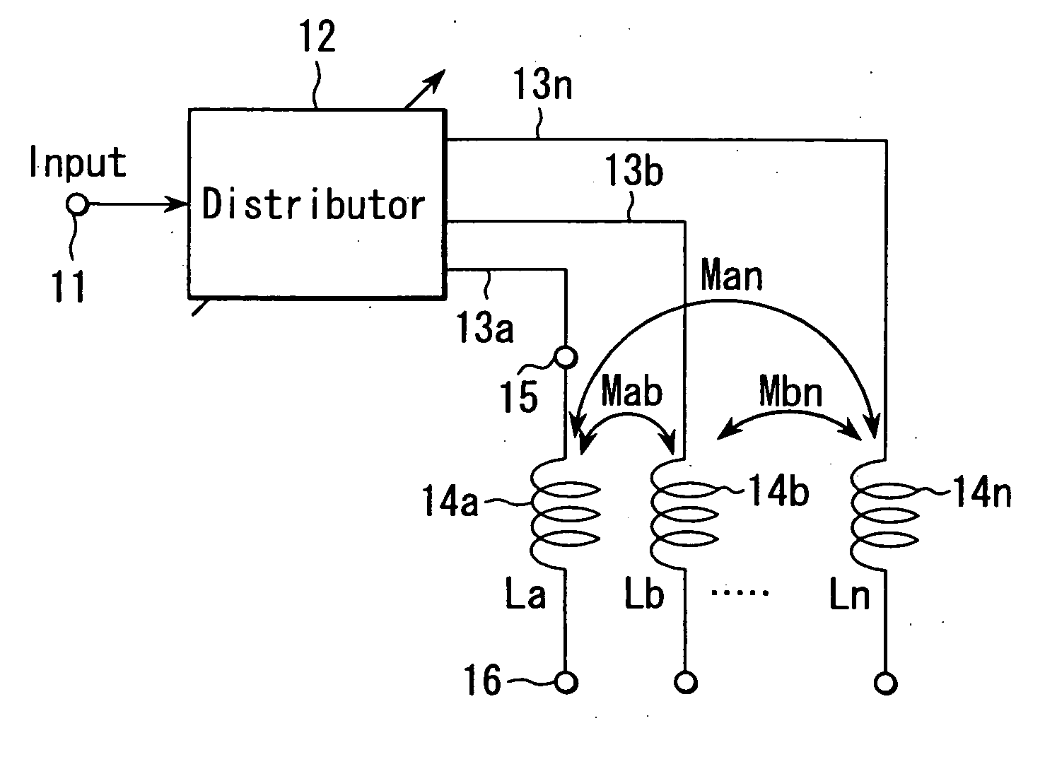
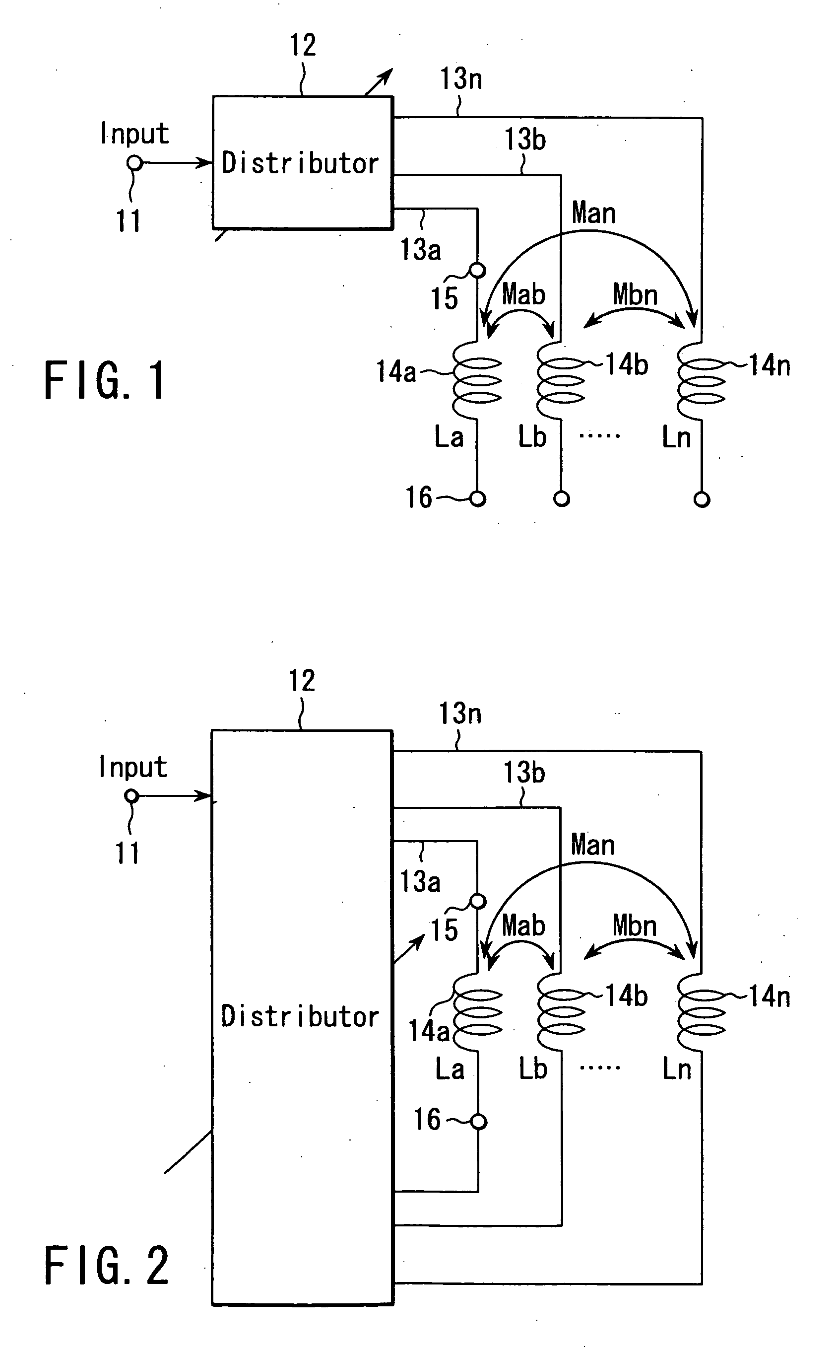
[0082] First, description will be made of a variable inductor according to a basic embodiment of the present invention. FIGS. 1 and 2 show circuitry of a viable inductor of a first embodiment of the present invention. An input signal (Input) input to a signal input terminal 11 is distributed to a plurality of signal paths 13a, 13b, . . . , 13n by a distributor 12 constituted by using an active element. Inductors 14a, 14b, . . . 14b are inserted into the signal paths 13a, 13b, . . . , 13n. The inductors 14a, 14b, . . . 14n are constituted of, e.g., spirally formed leads, and arranged close to one another to be interconnected.

[0083] The inductors 14a, 14b, . . . 14n generate magnetic fluxes depending on sizes of input signals, and each magnetic flux is applied on the other close inductor to interconnect each inductor with this other inductor. Thus, the inductors 14a, 14b, . . . 14n have self inductance caused by a magnetic flux generated by each inductor itself, and mutual inductance...

second embodiment

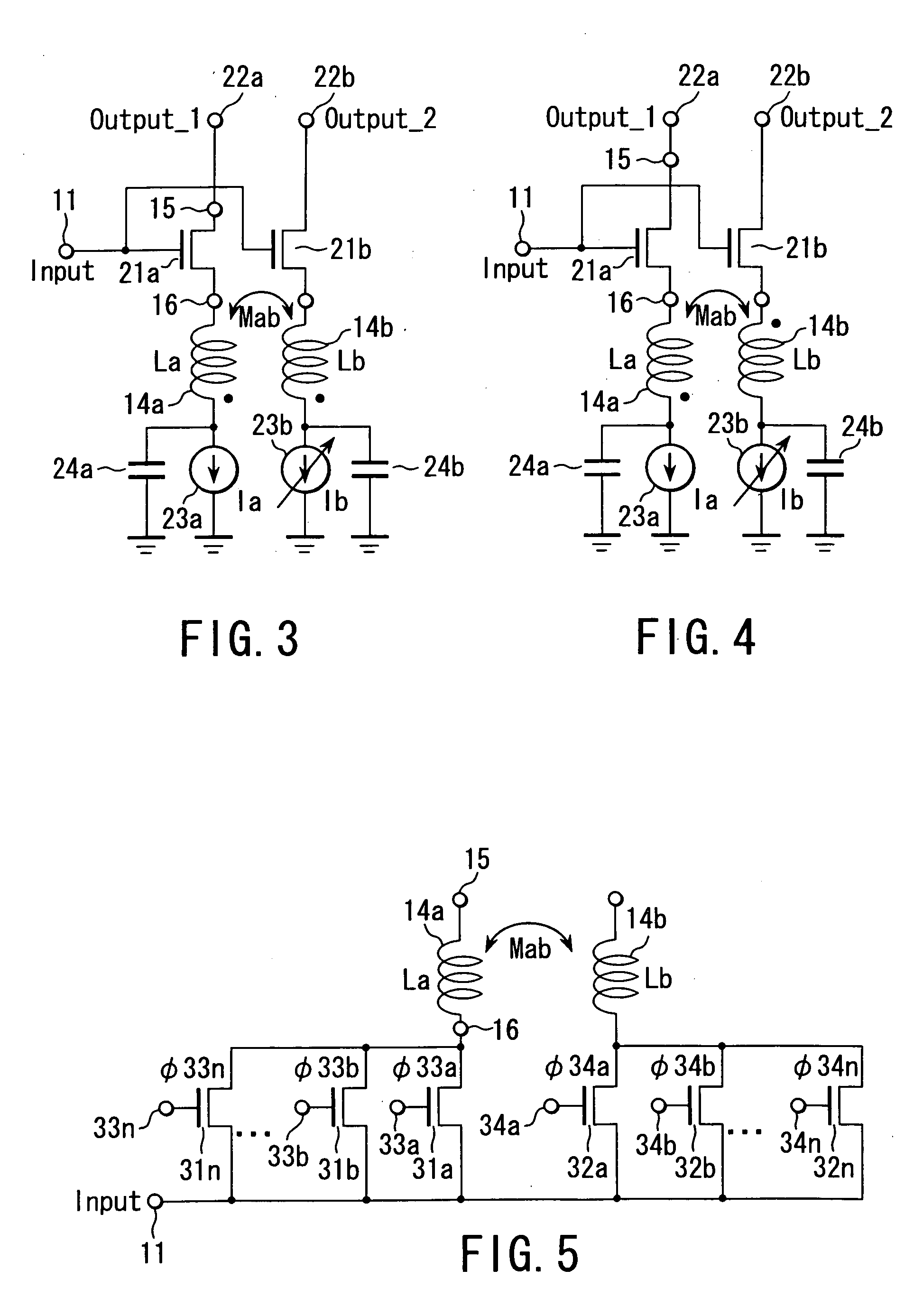
[0087]FIGS. 3 and 4 show a variable inductor where the distributor 12 includes a common source circuit according to the embodiment. The circuit of this embodiment is equivalent to the specific circuit example of the basic circuitry shown in FIG. 1. The input signal from the signal input terminal 11 is amplified by a common source circuit, e.g., MOSFET's (simply referred to as transistor, hereinafter) 21a, 21b to be distributed to two signal paths, and supplied to the inductors 14a, 14b inserted into these signal paths. Gate terminals of the transistors 21a, 21b are connected to the signal input terminal 11, source terminals are connected to ends of the inductors 14a, 14b, and drain terminals are connected to output terminals 22a, 22b of the variable inductor. In this variable inductor, signal currents amplified by the MOSFET's 21a, 21b are outputted from output terminals 22a, 22b of the variable inductor.

[0088] The other ends of the inductors 14a, 14b are connected to ends of power...

third embodiment

[0097]FIG. 5 shows a variable inductor according to a third embodiment which uses a transistor circuit where a gate is grounded to a distributor 12. A source terminal of at least one of first transistors 31a, 31b, . . . , 31n, and source terminals of a plurality of second transistors 32a, 32b, . . . , 32n are connected to a signal input terminal 11. Drain terminals of the first transistors 31a, 31b, . . . , 31n are connected to one end of a first inductor 14a, and gate terminals are connected to control signal input terminals 33a, 33b, . . . , 33n. Drain terminals of the second transistors 32a, 32b, . . . , 32c are connected in common to one end of a second inductor 14b, and gate terminals are connected to control signal input terminals 34a, 34b, . . . , 34n.

[0098] Control signals φ33a, φ33b, . . . , φ33n are input to the control signal input terminals 33a, 33b, . . . , 33c. Control signals φ34a, φ34b, . . . , φ34n are input to the control signal input terminals 34a, 34b, . . . , 3...


PUM


Abstract

An amplifier comprises an amplifier circuit which comprises a first inductor as an impedance element for degeneration, and a control circuit which has a second inductor electro-magnetically connected to the first inductor, and changes a control current flowing through the second inductor to change an inductance value of the first inductor, thereby changing amplification characteristics of the amplifier circuit.

Description

CROSS-REFERENCE TO RELATED APPLICATIONS [0001] This application is based upon and claims the benefit of priority from the prior Japanese Patent Applications No. 2002-160621, filed May 31, 2002; No. 2002-188946, filed Jun. 28, 2002; and No. 2002-270984, filed Sep. 18, 2002, the entire contents of all of which are incorporated herein by reference. BACKGROUND OF THE INVENTION [0002] 1. Field of the Invention [0003] This invention relates to a variable inductor, and more particularly to a variable inductor which uses a circuit constituted of an active element and a plurality of interconnected inductors to change inductance. [0004] Additionally, this invention relates to an oscillator having an inductor, and a radio terminal having an inductor, and also relates to improvements in a circuit designing technology of an amplifier and a radio terminal and a gain varying method of the amplifier. [0005] 2. Description of the Related Art [0006] Generally, in order to vary characteristics of an e...

Claims


Application Information

Patent Timeline
Patent Type & Authority Applications(United States)
IPC IPC(8): H03J7/02H03B5/12H03F3/45H03H11/48
CPCH03B5/1841H03B5/1271H03F3/45183H03F3/45188H03F3/72H03F2200/294H03F2200/372H03F2203/45318H03F2203/45362H03F2203/45386H03F2203/45591H03F2203/45638H03G1/0029H03H11/48H03J2200/10H03B5/1225H03B5/1228H03B5/1231H03B5/1296H03B5/1215H03B5/1243H03B5/1209H03B5/1278H03B5/1256H03F3/45089H03H11/485
Inventor FUJIMOTO, RYUICHIITAKURA, TETSURO
Owner KK TOSHIBA
Why Eureka
Try Eureka