Manufacturing method of semiconductor device

Inactive Publication Date: 2006-03-09
SEMICON ENERGY LAB CO LTD
View PDF28 Cites 31 Cited by
  • Summary
  • Abstract
  • Description
  • Claims
  • Application Information

AI Technical Summary

Benefits of technology

[0031] According to the present invention, since crystallization and gettering can be performed simultaneously, only one-time heat treatment step is required and the number of processes can be reduced dra

Problems solved by technology

However, in the case of using the crystalline semiconductor film obtained by this method, there is a risk of serious deterioration in TFT characteristics due to the catalytic element in the film.
Specifically, there is a possibility of in

Method used


Image

  • Manufacturing method of semiconductor device
  • Manufacturing method of semiconductor device
  • Manufacturing method of semiconductor device

Examples


Example

Embodiment 1

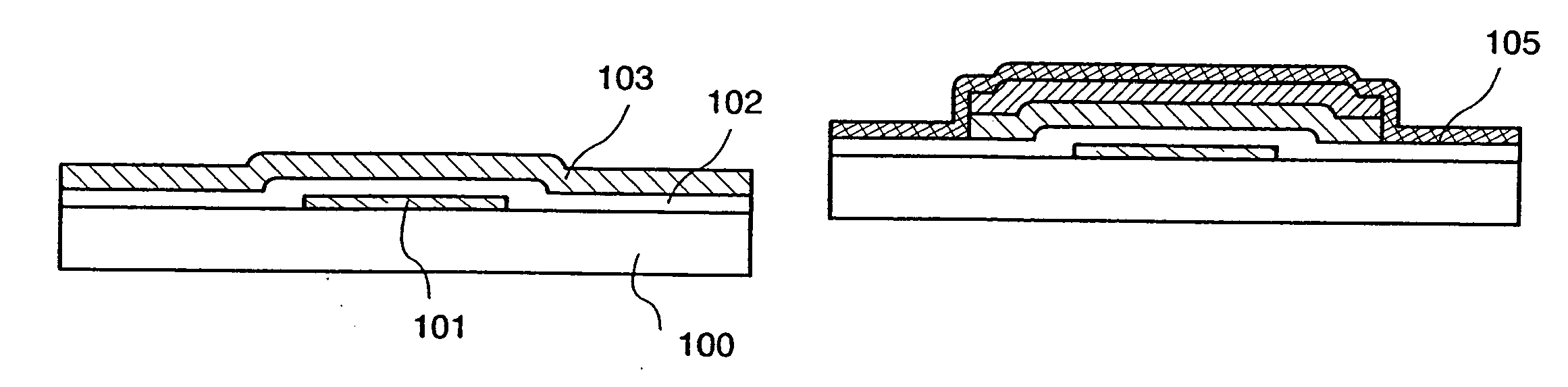
[0106] Embodiment 1 is described with reference to FIGS. 7A to 9C.

[0107] First, as shown in FIG. 7A, gate electrodes 501 to 503 are formed over a substrate 500. A glass substrate such as barium borosilicate glass or alumino borosilicate glass; a quartz substrate; a stainless steel substrate; or the like can be used as the substrate 500. In addition, a substrate formed from a synthetic resin having flexibility such as plastic typified by PET, PES, and PEN, or acrylic may be used as the substrate 500.

[0108] The gate electrodes 501 to 503 are formed to have a single layer structure of a conductive film or a stacked structure of two or more conductive films. When two or more conductive films are stacked, the gate electrodes 501 to 503 may be formed with a stacked layer of an element selected from tantalum (Ta), tungsten (W), titanium (Ti), and molybdenum (Mo); or an alloy material or a compound material containing the element as its main component. In addition, the gate e...

Example

Embodiment 2

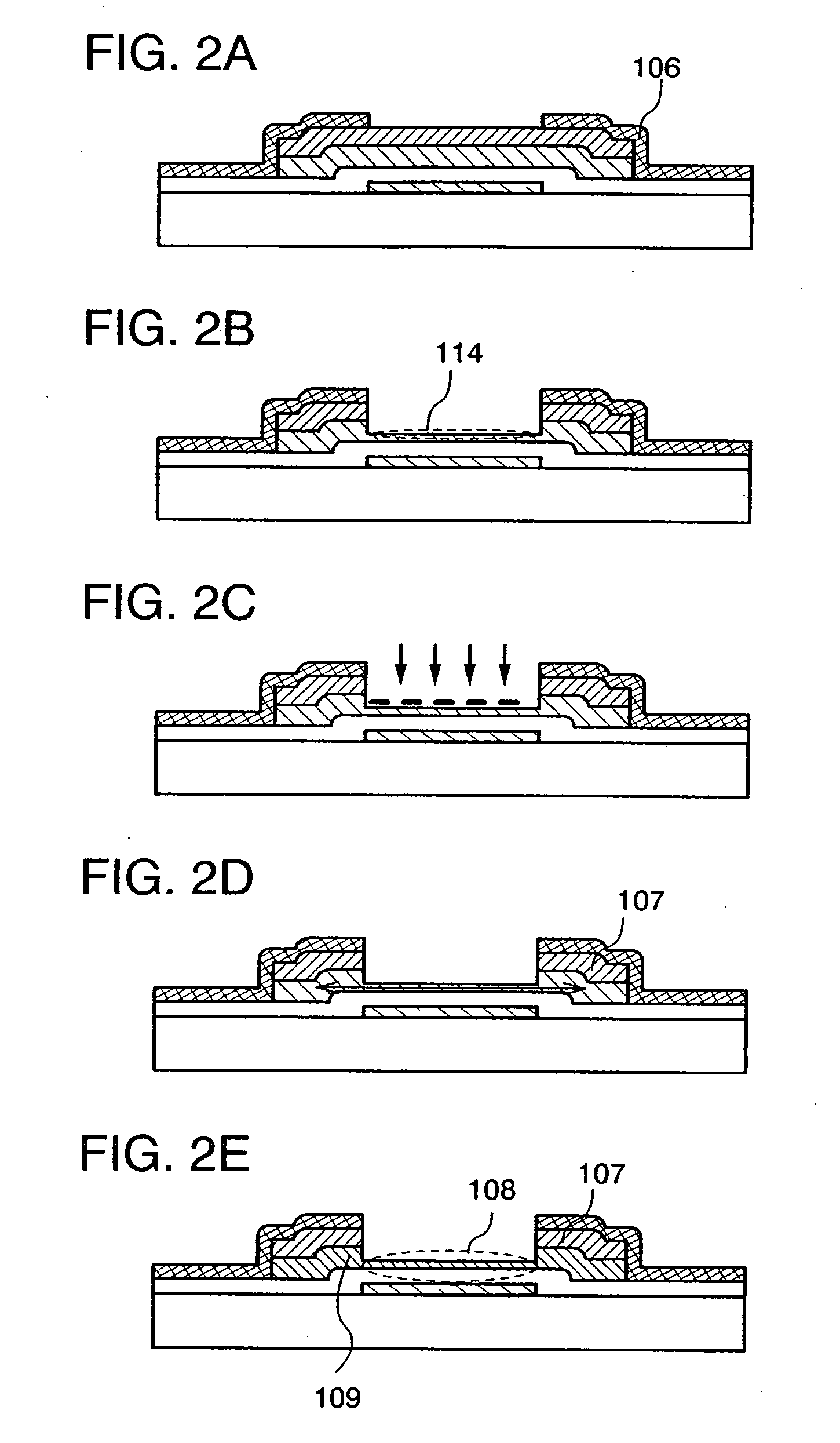
[0131] In Embodiment 2, an example of adding a catalytic element more selectively is described with reference to FIGS. 5A to 6B.

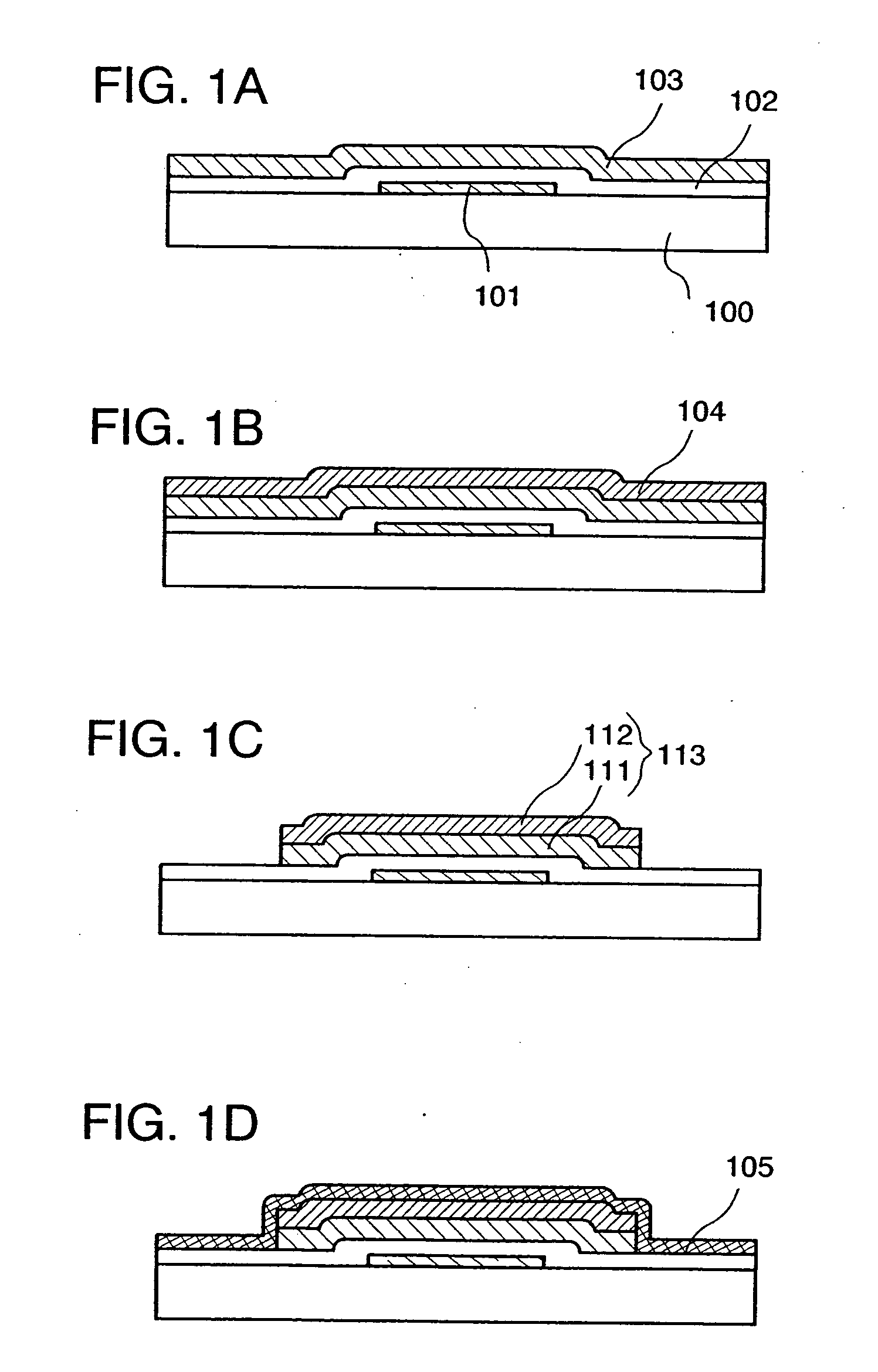
[0132] First, the process up to etching the island-shaped region 113 shown in FIG. 2B is performed according to the process described in Embodiment Mode. Note that the same portions as those in Embodiment Mode are denoted with the same reference numerals (FIG. 5A).

[0133] A mask 201 is formed to cover a region 114 in which a source region and / or a drain region 106 and an island-shaped amorphous semiconductor film 111 are exposed. The mask 201 may be formed using a heat-resistant material because a heat treatment is performed in a later process. For example, silicon oxide, silicon nitride, silicon nitride containing oxygen, or silicon oxide containing nitrogen is used. In this embodiment, the mask 201 is formed with silicon oxide. In addition, the mask 201 is etched to be provided with an opening 200 for adding a catalytic element over the regi...

Example

Embodiment 3

[0152] In Embodiment 3, an example of forming wirings connected to a source electrode and / or a drain electrode using a low melting point conductive material is described with reference to FIGS. 10A and 11.

[0153] First, the process up to forming the conductive film 105 shown in FIG. 1D is performed according to the process described in Embodiment Mode. Note that the same portions as those in Embodiment Mode are denoted with the same reference numerals (FIG. 10A).

[0154] A resist mask is formed over the conductive film 105, and the conductive film 105 is patterned to form a source electrode and / or a drain electrode 301. However, wirings are formed in a later process separately from the source electrode and / or the drain electrode 301. Only the source electrode and / or the drain electrode 301 is formed in this process (FIG. 10B).

[0155] An island-shaped region 113 is etched using the source electrode and / or the drain electrode 301 as a mask. The etching method described in ...


PUM


Abstract

An amorphous semiconductor film and a semiconductor film including an element selected from Group 15 of the periodic table are formed over a substrate. An island-shaped region including an island-shaped amorphous semiconductor film and an island-shaped semiconductor film is formed. A source electrode and a drain electrode are formed over the island-shaped region. The island-shaped semiconductor film that is not covered by the source electrode and the drain electrode is removed using the source electrode and the drain electrode as a mask. At this time, the thickness of the island-shaped amorphous semiconductor film is reduced, and a portion of the island-shaped amorphous semiconductor film is exposed. A catalytic element promoting crystallization is added into a region in which the island-shaped amorphous semiconductor film is exposed. By a heat treatment, the island-shaped amorphous semiconductor film is crystallized and the catalytic element is gettered.

Description

BACKGROUND OF THE INVENTION [0001] 1. Field of the Invention [0002] The present invention relates to a semiconductor element such as a thin film transistor (hereinafter, referred to as a TFT) and a method for manufacturing a semiconductor device having a circuit including such a semiconductor element. For example, the present invention relates to an electro-optical device typified by a liquid crystal display, an EL (electroluminescense) display device, an EC display device, and the like. The present invention also relates to an electrical unit for improving processing speed formed using a TFT, for example, a central processing unit (CPU), and the manufacturing method thereof. Further, the present invention relates to an electronic device with the electro-optical device and the electrical unit mounted as a part. [0003] 2. Description of the Related Art [0004] Recently, the technique for manufacturing a semiconductor element such as a TFT over a substrate has improved drastically and ...

Claims


Application Information

Patent Timeline
IPC IPC(8): H01L21/8234H01L21/336
CPCH01L21/2022H01L27/12H01L27/1277H01L29/66765H01L27/1292H01L27/1266H01L21/02672H01L21/3221H01L27/1214
Inventor KAKEHATA, TETSUYATAKEHARA, YUUICHIJINBO, YASUHIRO
Owner SEMICON ENERGY LAB CO LTD
Why Eureka
Try Eureka