
Discharge-processing power source device

a power source device and discharge processing technology, applied in the direction of electric variable regulation, instruments, manufacturing tools, etc., can solve the problems of high cost of cooling of elements, inability to perform high-speed operations of switching elements, and large space occupation of elements in circuits, so as to reduce the number of elements and increase the current

Inactive Publication Date: 2006-03-16
MITSUBISHI ELECTRIC CORP
View PDF3 Cites 13 Cited by
  • Summary
  • Abstract
  • Description
  • Claims
  • Application Information

AI Technical Summary

Benefits of technology

[0052] According to the present invention, the switching circuit including switching elements suitable for a high-speed operation and the switching circuit including switching elements suitable for a low-speed operation can be driven sequentially such that a discharge current continues in an identical discharge current pulse generation time. Thus, a large and high-frequency intermittent discharge current can be generated. Therefore, wire electric discharge machining coping with a large current and a high frequency can be performed efficiently. In addition, since the switching elements with different characteristics are used, the number of elements can be reduced. As a result, a heat value can be reduced.
[0054] According to the present invention, the first switching circuit performs switching faster than the second switching circuit by a time equivalent to a processing time for generating a control pulse signal. Therefore, a faster operation can be realized. In addition, since the first switching circuit can use both the switching elements suitable for a high-speed operation and the switching elements suitable for a low-speed operation, a range of selection of elements to be used can be widened.
[0060] According to the present invention, a circulating current drive system with large input energy per one pulse of intermittent discharge can be realized using the switching circuit including a switching element suitable for a low-speed operation. Therefore, wire electric discharge machining using a thick wire electrode requiring a large current becomes possible.
[0072] According to the present invention, the switching circuit suitable for a low-speed operation can be actuated at the time of normal discharge when a large current is applied, and the switching circuit suitable for a high-speed operation can be actuated at the time of short circuit or immediate discharge when a repetition frequency increases. Therefore, wire electric discharge machining coping with a large current and a high frequency can be performed efficiently. In addition, since the switching elements with different characteristics are used, the number of elements can be reduced, and as a result, a heat value can be reduced. Moreover, since a repetition frequency of the switching circuit on the low-loss side can be controlled to ½ to ⅓, an element with a larger current and a lower loss (e.g., IGBT) can be used.
[0074] According to the present invention, both the switching circuit suitable for a high-speed operation and the switching circuit suitable for a low-speed operation can be actuated at the time of normal discharge when a large current is applied, and only the switching circuit suitable for a high-speed operation can be actuated at the time of short circuit or immediate discharge when a repetition frequency increases. Therefore, wire electric discharge machining coping with a large current and a high frequency can be performed efficiently. In addition, since the switching elements with different characteristics are used, the number of elements can be reduced, and as a result, a heat value can be reduced. Moreover, since a repetition frequency of the switching circuit on the low-loss side can be controlled to ½ to ⅓, an element with a larger current and a lower loss (e.g., IGBT) can be used.

Problems solved by technology

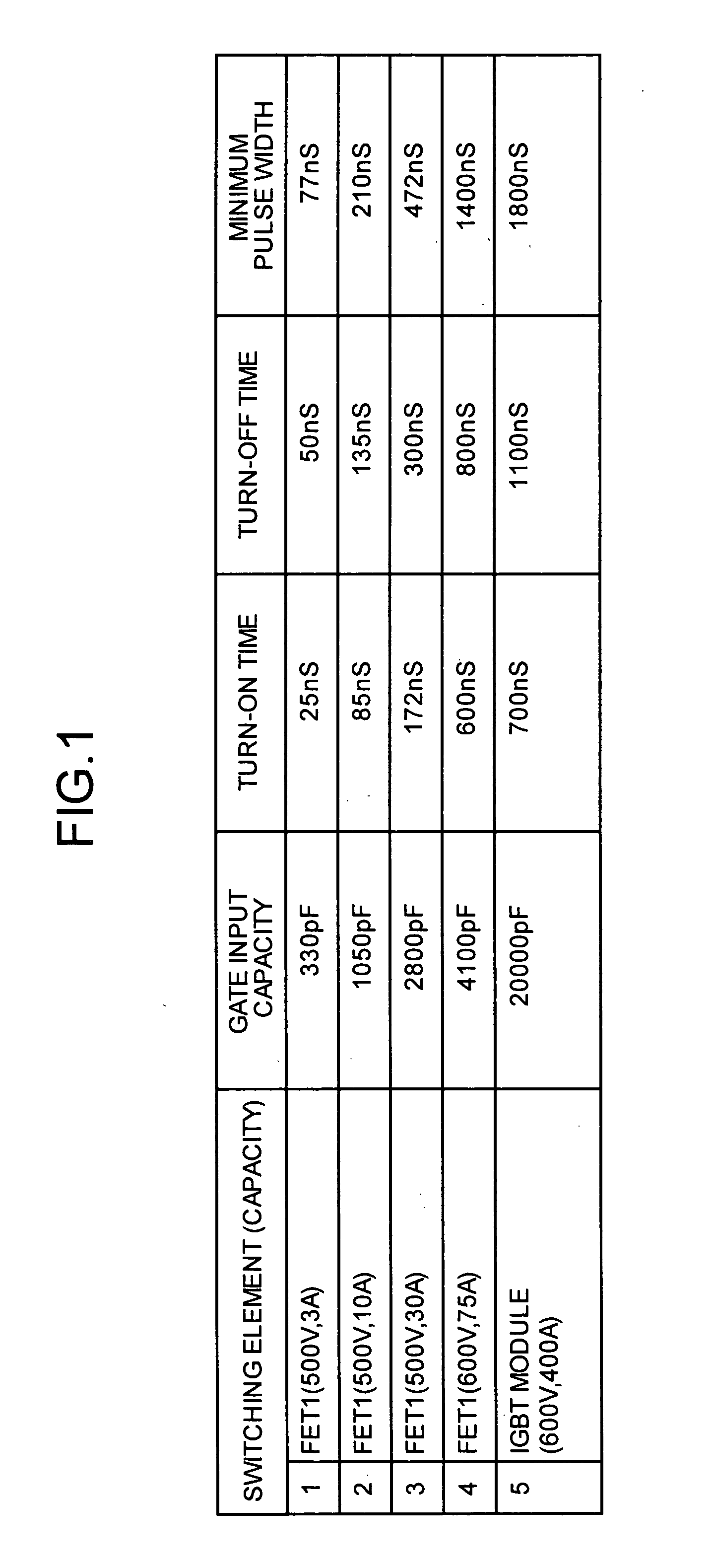
Since an element having a small ON resistance and small heat generation among the switching elements has a large gate input capacity, the switching element cannot perform a high-speed operation.
In addition, since an element having a small gate input capacity and capable of performing a high-speed operation has a large ON resistance and a small maximum current capacity and also has a large heat value, there is a problem in that, for example, cooling of the element is costly and the element occupies a large space.
In this case, elements in the circuit are likely to be destroyed due to a potential difference including a surge voltage.
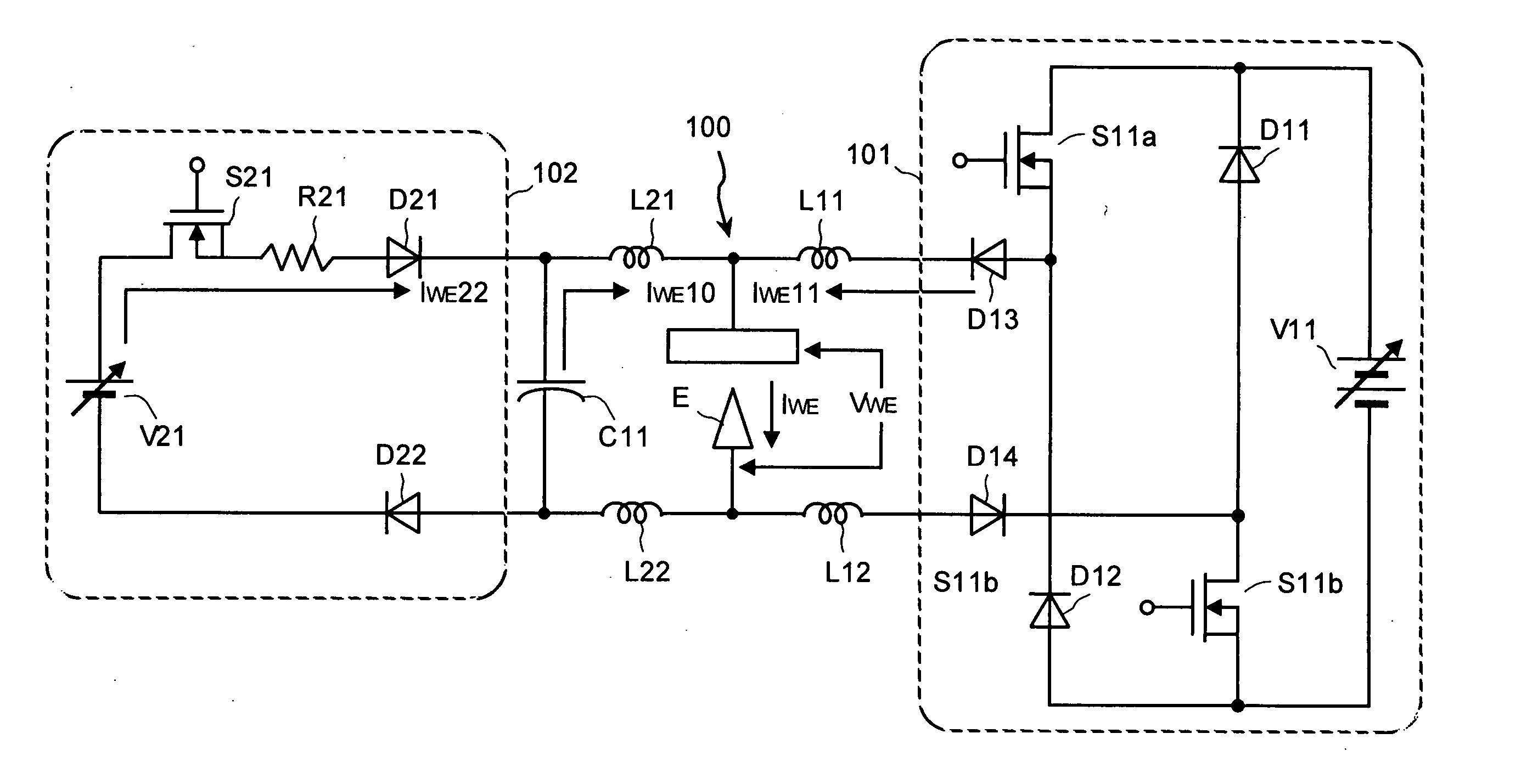
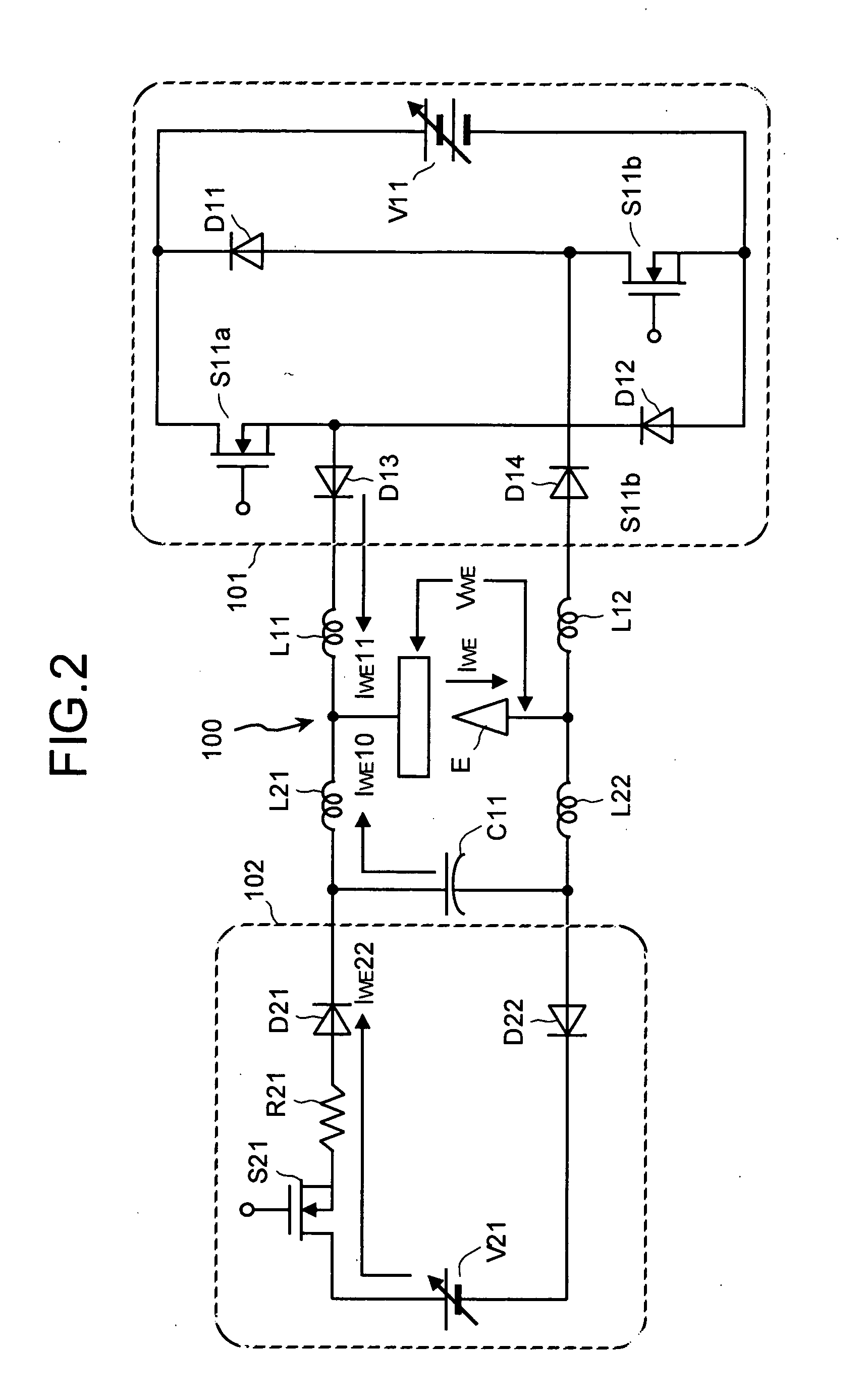
However, in the conventional power supply device for electric discharge machining, an upper limit value of the discharge maintenance current IWE22 is limited by the resistor R21.
Therefore, there is a problem in that the conductive path in the inter-electrode portion formed after occurrence of discharge cannot be maintained, and input of the electric discharge machining current IWE11 fails.
Thus, various failures occur in electric discharge machining.
As a result, there is a problem in that machining speed, which should be obtained originally, cannot be obtained, and further improvement of the machining speed cannot be realized.
As a result, when a wire electrode is thin, the wire electrode is broken.
Even if breakage does not occur in the wire electrode, there is a problem in that, for example, a machining surface is roughened, machining accuracy is deteriorated, and stable electric discharge machining characteristics cannot be obtained.
However, in this measure, since an excess capacitor is added in the inter-electrode portion eventually, for example, an electric capacitance viewed from a power supply device side increases according to a stray capacitance in the circuit, a rising time constant at the time when an output voltage is applied to the inter-electrode portion increases, and rising of an inter-electrode voltage is delayed.
Consequently, since a voltage application time until discharge is caused becomes long, there is a disadvantage in that the number of times of effective discharge decreases and the machining efficiency cannot be improved sufficiently.
A dielectric loss is present even in a capacitor for a high-frequency application.
H5-9209, in addition to a problem of limiting the oscillation frequency of voltage application, there is also a problem in that heat generation occurs due to the dielectric loss, and a loss of supply energy is also caused.

Method used


Image

  • Discharge-processing power source device
  • Discharge-processing power source device
  • Discharge-processing power source device

Examples


first embodiment

[0100]FIG. 5 is a circuit diagram of a main structure of a power supply device for electric discharge machining that is a first embodiment of the present invention. FIG. 6 is a block diagram of a structure of a power supply circuit that controls to drive switching elements of the power supply device for electric discharge machining shown in FIG. 5.

[0101] In FIG. 5, an electrode E and a workpiece W are arranged at an appropriate interval in an electric discharge machining unit. A DC voltage (inter-electrode voltage) can be applied between the electrode E and the workpiece W from the outside at the time when discharge is started. Note that a stray capacitance C1 is present between the electrode E and the workpiece W.

[0102] A variable DC power supply V1, switching elements Sa1, S1b, S2a, and S2b, and diodes D1 and D2 are arranged with respect to the electrode E and the workpiece W. Here, an element suitable for a large current and a low-loss (e.g., IGBT) is used for the switching ele...

second embodiment

[0135]FIG. 10 is a block diagram of a structure of a power supply control circuit included in a power supply device for electric discharge machining that is a second embodiment of the present invention. Note that, in FIG. 10, components identical with or equivalent to the components described in the first embodiment (FIG. 6) are denoted by the identical reference numerals and signs. Here, parts related to the second embodiment will be mainly explained.

[0136] In short, the power supply control circuit according to the second embodiment is a circuit that controls to drive the switching elements S1a, S1b, S2a, and S2b in the power supply device for electric discharge machining described in the first embodiment (FIG. 1). In the second embodiment, as a relation of characteristics between the switching elements S1a and S1b and the switching elements S2a and S2b, a speed difference may be large as in the first embodiment. However, the second embodiment can be applied even when the speed d...

third embodiment

[0160]FIG. 13 is a block diagram of a structure of a power supply control circuit included in a power supply device for electric discharge machining that is a third embodiment of the present invention. Note that, in FIG. 10, components identical with or equivalent to the components described in the second embodiment (FIG. 10) are denoted by the identical reference numerals and signs. Here, parts related to the third embodiment will be mainly explained.

[0161] In short, the power supply control circuit according to the third embodiment is a circuit that controls to drive the switching elements S1a, S1b, S2a, and S2b in the power supply device for electric discharge machining described in the first embodiment (FIG. 1). As shown in FIG. 13, drive circuits 7a and 7b, a numerical control device 8, and a switching device 9 are added as components in addition to the components described in the second embodiment (FIG. 10).

[0162] An input signal of the drive circuits 7a and 7b is the start ...


PUM

PropertyMeasurementUnit
Widthaaaaaaaaaa

Abstract

A power supply device for electric discharge machining includes a switching circuit that supplies a discharge pulse current to an inter-electrode portion that is a portion between an electrode and a workpiece serving as another electrode arranged to be opposed to the electrode at a predetermined interval; and a pulse-width control unit that generates a control pulse signal of a predetermined pulse width in response to a detection signal for starting a discharge at the inter-electrode portion. The switching circuit includes a switching circuit including a switching element suitable for a high-speed operation and a switching circuit including a switching element suitable for a low-speed operation, and receives the control pulse signal in parallel.

Description

TECHNICAL FIELD [0001] The present invention relates to a power supply device for electric discharge machining used in a wire electric discharge machining apparatus that causes electric discharge between a wire electrode and a workpiece serving as the other electrode (hereinafter referred to as “inter-electrode portion”) to subject the workpiece to wire electric discharge machining, and more particularly, to a power supply device for electric discharge machining used in a wire electric discharge machining apparatus that performs wire electric discharge machining compliant with a large current and a high frequency. BACKGROUND ART [0002] (Publicly-Known Technique Concerning Wire Electric Discharge Machining) [0003] It is a well-known technique that wire electric discharge machining can be performed at high speed while preventing breaking of wire by applying large and small current pulses to an inter-electrode portion according to a state of the inter-electrode portion represented by a...

Claims


Application Information

Patent Timeline
IPC IPC(8): B23H1/02B23H7/14
CPCB23H2300/20B23H1/022
Inventor SATOU, SEIJIOOGURO, HIROYUKI
Owner MITSUBISHI ELECTRIC CORP
Learn More