Organic semiconductor structure, manufacturing method of the same, and organic semiconductor device

a manufacturing method and semiconductor technology, applied in the direction of solid-state devices, transistors, thermoelectric devices, etc., can solve the problems of difficult formation of organic semiconductor layers, grain boundaries and defects inhibiting charge transportation, and easily occurring defects, etc., to achieve fewer structural defects and easy to obtain large area

Inactive Publication Date: 2006-03-23
DAI NIPPON PRINTING CO LTD
View PDF2 Cites 10 Cited by
  • Summary
  • Abstract
  • Description
  • Claims
  • Application Information

AI Technical Summary

Benefits of technology

[0022] According to the manufacturing method of organic semiconductor structure of the present invention, since an organic semiconductor layer comprising a large crystal with few structural defects can be formed, the charge transport property of the organic semiconductor layer can be uniformalized over a large area. Moreover, the organic semiconductor layer can be formed into a shape according to a previously designed lipophilic region pattern depending on electric circuits or organic semiconductor device. Further, since the organic semiconductor layer can be formed by coating a solution of an organic semiconductor material, it is easy to form organic semiconductor layer having uniform charge transport property over a large area.
[0023] According to the organic semiconductor structure and the organic semiconductor device of the present invention, since the organic semiconductor layer having uniform charge transport property over a large area can be obtained easily, this can contribute greatly to realization of a thin film-large area device.

Problems solved by technology

However, generally in the organic semiconductor layers formed by the above-mentioned vacuum deposition process, a large number of grain boundaries easily occur in polycrystal state of aggregated fine crystals, and further, defects easily occur so that such grain boundaries and defects inhibit transportation of charge.
Accordingly, when an organic semiconductor layer is formed by vacuum deposition process, it is actually very difficult to form an organic semiconductor layer serving as an element of an organic semiconductor device continuously with uniform performance over a sufficiently large area.
Thus, there is a problem that it is difficult to apply industrially because strict control of molecular alignment is required.
Up to now, there is no report on a successful example of a thin-film transistor using the discotic liquid crystal as a material of an organic semiconductor layer.
However, there is still no report on a successful example of a thin-film transistor using the rod-shaped liquid crystal material in an organic semiconductor layer.
However, when this liquid crystal material is transferred into a crystal state of higher structural regularity, the mobility of charge is reversely decreased or not observed, thus naturally failing to exhibit the performance of a thin-film transistor.
However, the charge carrier mobility of the resulting organic semiconductor layer is as low as 10−5 to 10−6 cm2 / V·s, and is problematic because of its dependency on temperature and electric field.

Method used


Image

  • Organic semiconductor structure, manufacturing method of the same, and organic semiconductor device
  • Organic semiconductor structure, manufacturing method of the same, and organic semiconductor device
  • Organic semiconductor structure, manufacturing method of the same, and organic semiconductor device

Examples


example 1

[0076] By using a phenyl naphthalene derivative (2-(4′-pentylphenyl)-6-metyloxynaphthalene. Hereinafter, this may be abbreviated as 5-PNP-O1.), which is the compound shown in the above chemical formula 39, as the organic semiconductor material, the organic semiconductor device was prepared. Moreover, using this material as an organic semiconductor material, an organic semiconductor layer was prepared and each property evaluation was carried out.

(Preparation of Organic Semiconductor Device)

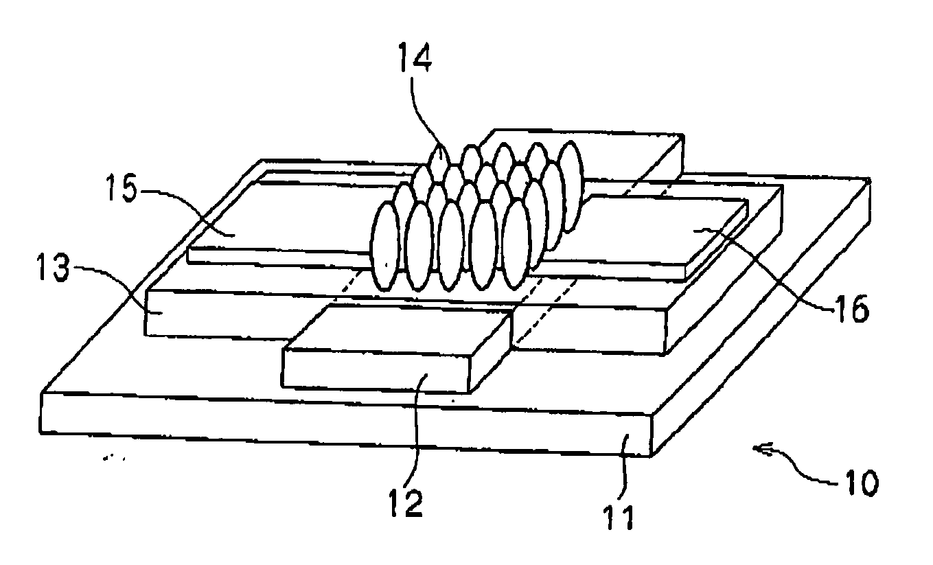
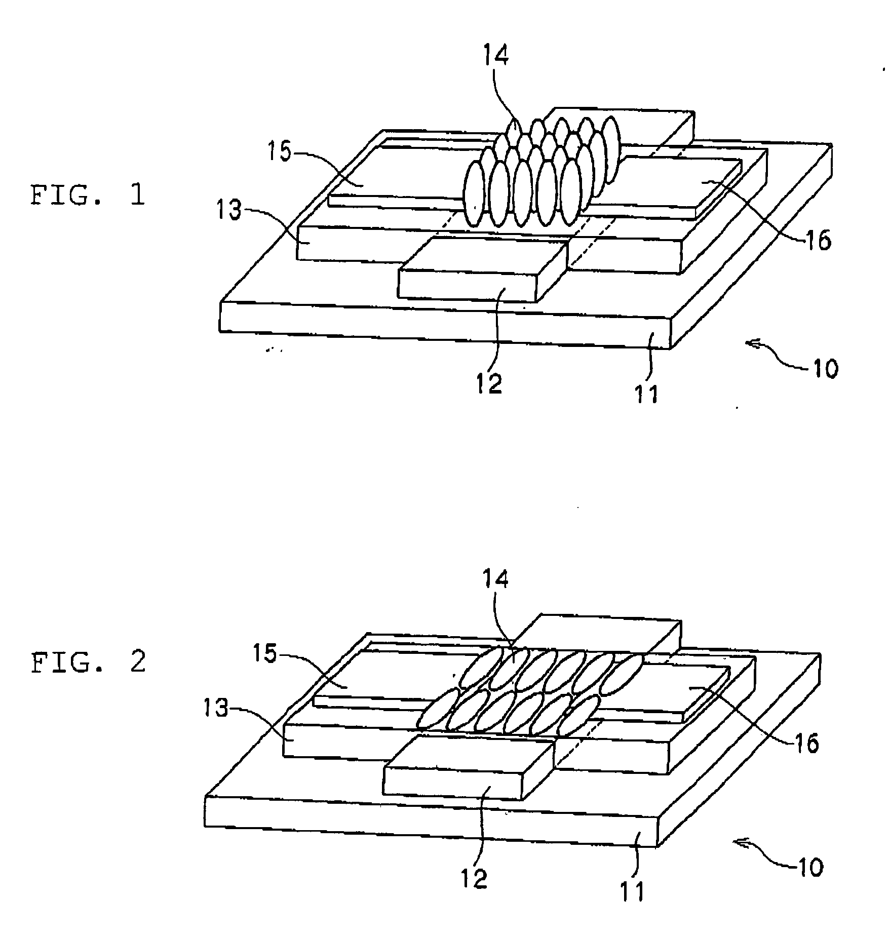
[0077] By using the above-described 5-PNP-O1 as an organic semiconductor material, the organic semiconductor device of Example 1 comprising substrate / gate electrode / gate-insulating layer on which a lipophilic region pattern and an oil repellent region pattern are formed (also serving as an liquid crystal alignment layer) / source-drain electrodes / organic semiconductor layer ( / protective layer) was prepared. [0078] A glass substrate (thickness: 1.1 mm, Corning 1737) subjected to ultrasonic cleaning...

example 2

[0102] For the organic semiconductor layer in Example 2 in which a phenyl naphthalene derivative (2-(4′-octylphenyl)-6-dodecyloxynaphthalene. Hereinafter, this may be abbreviated as 8-PNP-O12.), which is the compound shown in the above chemical formula 40, is used as the organic semiconductor material, each property evaluation as similar to Example 1 was carried out.

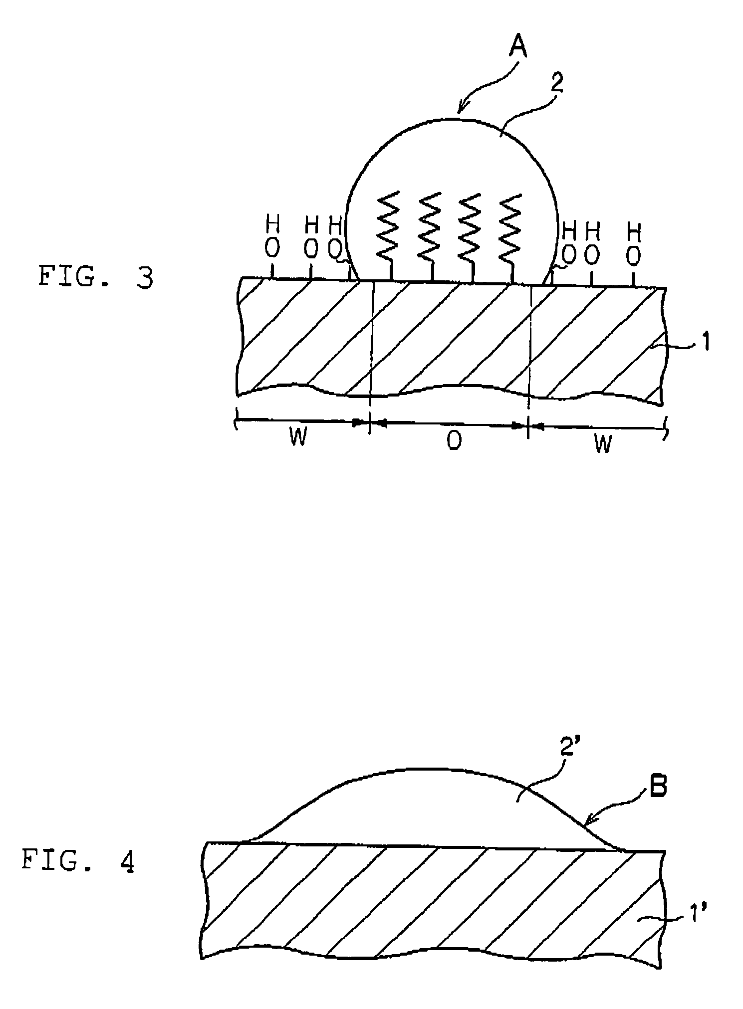
[0103] The organic semiconductor layer for evaluation of charge carrier mobility and evaluation of structure defect density was prepared by using 4 mm×100 mm rectangle pattern as a mask pattern; subjecting a glass substrate, on which a comb shaped Au electrode (between the comb L=200 μm, comb width W=28 mm) is formed, to the similar treatment as the forming treatment of a lipophilic region pattern and an oil repellent region pattern in the above-described preparation of organic semiconductor device in Example 1; dropping 1 wt % p-xylene solution of 8-PNP-O12 to the lipophilic region on the glass substrate, at atmosphere...


PUM


Abstract

The main object is to provide a manufacturing method of organic semiconductor, an organic semiconductor device structure manufactured by the manufacturing method and an organic semiconductor device, those having uniform and high carrier transport property over a relatively large area. To achieve the object, the present invention provides a manufacturing method of an organic semiconductor structure, wherein the organic semiconductor structure comprises, on a base material, an organic semiconductor layer formed from a liquid crystalline organic semiconductor material, and comprising processes of: forming an oil repellent region and a lipophilic region, which is surrounded by the oil repellent region, on the base material; coating an organic semiconductor layer forming solution, comprising the liquid crystalline organic semiconductor material and a solvent, on the lipophilic region; and crystallizing the liquid crystalline organic semiconductor material by evaporating the solvent in the organic semiconductor layer forming solution coated on the lipophilic region.

Description

BACKGROUND OF THE INVENTION [0001] 1. Field of the Invention [0002] The present invention relates to a manufacturing method of an organic semiconductor structure, wherein the organic semiconductor structure comprising an organic semiconductor layer formed with organic semiconductor material having liquid crystallinity, an organic semiconductor structure manufactured by the manufacturing method of and an organic semiconductor device. [0003] 2. Description of the Related Art [0004] As a typical example of an organic semiconductor device, an organic field-effect transistor (also called organic FET) using an organic semiconductor as an active layer (hereinafter, referred to as an organic semiconductor layer) can be mentioned. In order to realize a thin film-large area device, the organic FET is required to have uniform charge carrier transport property and high carrier mobility over a sufficient large area. [0005] In this organic FET, the organic semiconductor layer is formed, by vacuum...

Claims


Application Information

Patent Timeline
Patent Type & Authority Applications(United States)
IPC IPC(8): H01L29/08H01L21/336H01L21/208H01L29/786H01L51/00H01L51/05
CPCH01L51/0004H01L51/0545H01L51/0076H10K71/13H10K85/731H10K10/466
Inventor HANNA, JUNICHIIINO, HIROAKIMAEDA, HIROKI
Owner DAI NIPPON PRINTING CO LTD
Why Eureka
Try Eureka