Low-noise semiconductor photodetectors

Inactive Publication Date: 2006-03-23
INFRARED NEWCO
View PDF4 Cites 8 Cited by
  • Summary
  • Abstract
  • Description
  • Claims
  • Application Information

AI Technical Summary

Benefits of technology

[0012] In accordance with the invention, a low noise photodetector comprises a body of semiconductor material substantially surrounded by dielectric material. A portion of the body surface is passivated by a high quality dielectric and a portion is unpassivated. The semiconductor body includes a p-n junction for operation as a photodetector to minimize leakage, the p-n junction (including its depletion region) intersects the semiconductor surface within the passivated portion of the surface, and leakage from the unpassivated surface is minimized by one or more of the following: 1) the body includes opposite polarity p-n junctions (n-p and p-n) in the electrical path between the surface and the photocurrent collector, 2) the body includes a highly doped region in contact with the dielectric, 3) a doped semiconductor outside a thin dielectric provides a charge accumulation region adjacent the interface.

Problems solved by technology

Surface leakage is caused by traps at the interface between the semiconductor and any dielectric surfaces which contact it.
In both cases, leakage will arise whenever an electron-hole pair is generated at a trap on the surface, and the electron and hole make their way to different junctions, causing current to flow in an external circuit.
A semiconductor photodetector using the photoelectric effect, such as a P-N photodiode, cannot avoid having a depletion layer intersecting the semiconductor surface.
The larger the depletion layer, the more surface leakage.
The un-depleted surfaces will also give rise to leakage current even if some means is found to suppress leakage at the depleted surface.
Germanium photodiodes have been reported to have undesirably high dark current for many applications.
This is approximately equal to the photocurrent that would be generated by bright sunlight, and represents a high level of leakage.
Germanium photodiodes formed in bulk germanium have reported leakage 10-100 times lower [3][4], but this is still not sufficient for imaging indoors or in twilight conditions.

Method used


Image

  • Low-noise semiconductor photodetectors
  • Low-noise semiconductor photodetectors
  • Low-noise semiconductor photodetectors

Examples


Embodiment Construction

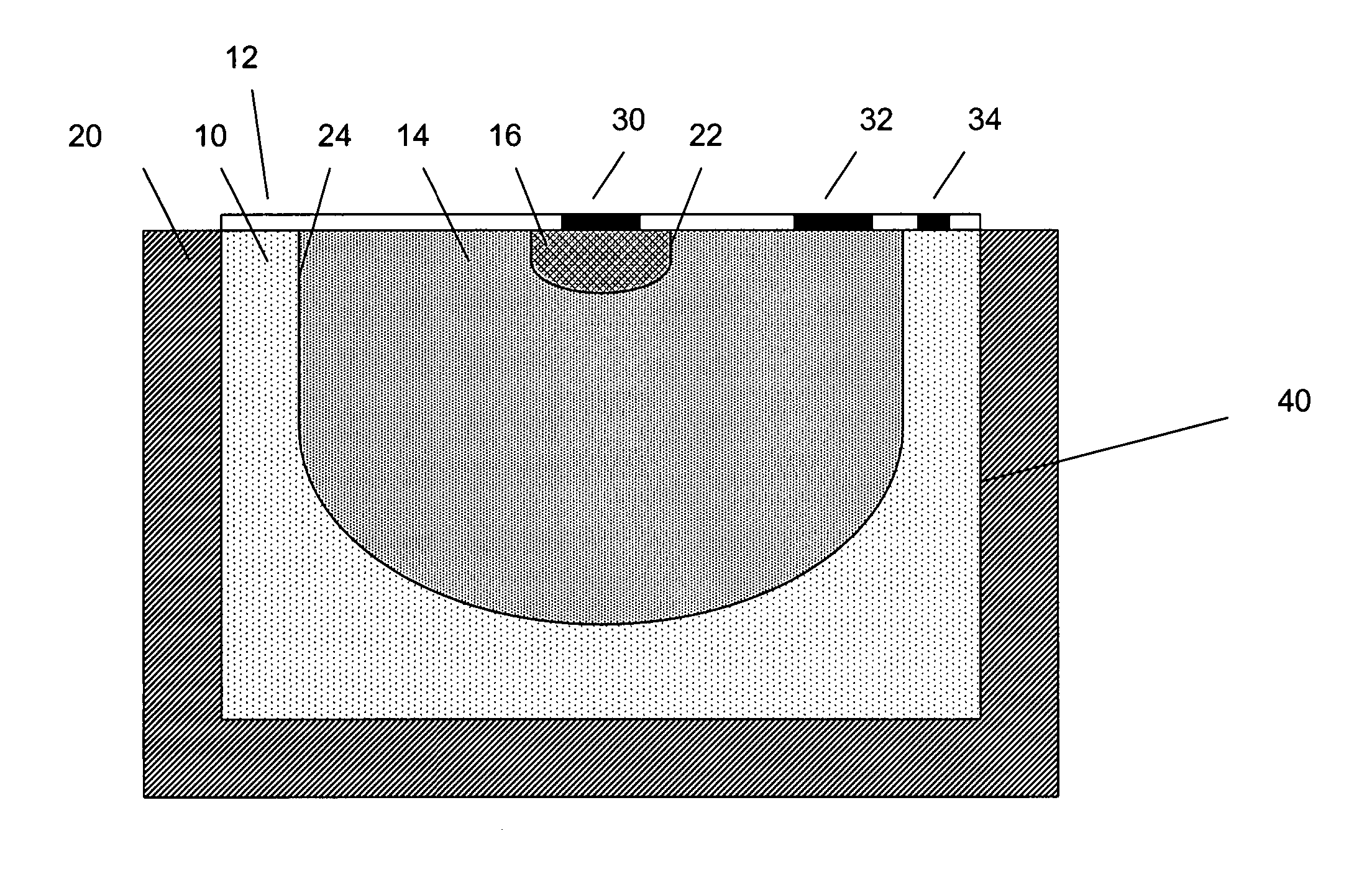
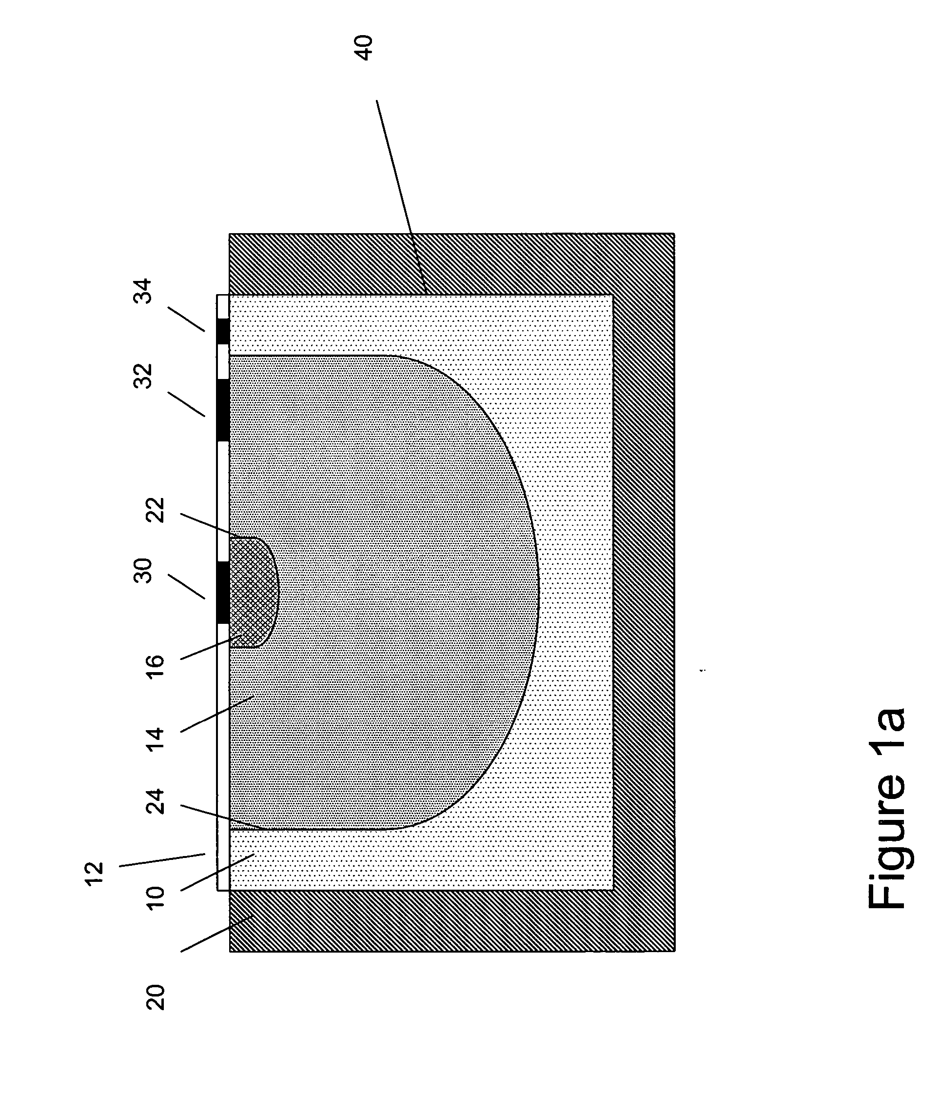
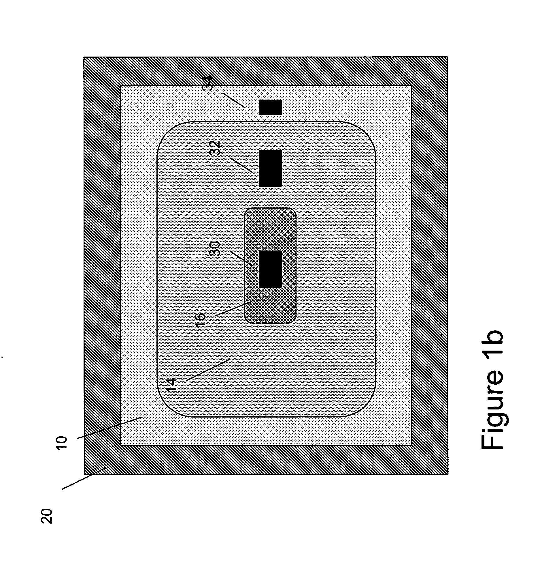
[0025]FIGS. 1a (cross-section) and 1b (plan-view) illustrate a low noise semiconductor photodetector. The semiconductor body 10 is substantially surrounded by dielectric material or materials. A first portion of the semiconductor surface is passivated, and a second portion is unpassivated. Here a high-quality dielectric 12 with a low surface recombination velocity is formed on the top surface of the semiconductor body 10 to passivate the top surface. The body is peripherally surrounded by low quality dielectric 20 that does not passivate the peripheral surface. The semiconductor body 10 is doped p-type. An n-type area 14 is formed in the body, peripherally enclosed by the p-type layer and forming a junction 24 between the n-type and p-type layer. A second p-type layer 16 is formed in the n-type layer 14, peripherally enclosed by the n-type layer and forming a junction 22 between the inner p-type and n-type layers (16,14). Ohmic metal contacts 30, 32, and 34 are formed to all the dop...


PUM


Abstract

A photodetector is formed from a body of semiconductor material substantially surrounded by dielectric surfaces. A passivation process is applied to at least one surface to reduce the rate of carrier generation and recombination on that surface. Photocurrent is read out from at least one electrical contact, which is formed on a doped region whose surface lies entirely on a passivated surface. Unwanted leakage current from un-passivated surfaces is reduced through one of the following methods. (a) The un-passivated surface is separated from the photo-collecting contact by at least two junctions (b) The un-passivated surface is doped to a very high level, at least equal to the conduction band or valence band density of states of the semiconductor (c) An accumulation or inversion layer is formed on the un-passivated surface by the application of an electric field. Electrical contacts are made to all doped regions, and bias is applied so that a reverse bias is maintained across all junctions.

Description

CROSS-REFERENCE TO RELATED APPLICATIONS [0001] This application is a continuation-in-part of U.S. patent application Ser. No. 10 / 453,037 filed by J. Bude et al. on Jun. 3, 2003 and entitled “Semiconductor Devices with Reduced Active Region Defects and Unique Contacting Schemes” which in turn claims the benefit of U.S. Provisional Application Ser. No. 60 / 434,359 filed by J. Bude et al on Dec. 18, 2002. Each of the foregoing applications, Ser. Nos. 10 / 453,037 and 60 / 434,359, are incorporated herein by reference.STATEMENT OF GOVERNMENT INTEREST [0002] The United States Government has certain rights to this invention pursuant to NSF Award DMI-0450487.FIELD OF INVENTION [0003] This invention relates to semiconductor photodetectors for visible and infrared light, and in particular, to low-noise semiconductor photodetectors and methods for making them. BACKGROUND OF THE INVENTION [0004] Semiconductor photodiodes are widely used for the detection of light, both visible and infrared. They ex...

Claims


Application Information

Patent Timeline
IPC IPC(8): H01L21/00H01L31/0232H01L21/20H01L27/146
CPCH01L27/14649H01L31/0352H01L31/03529H01L31/101H01L2924/0002Y02E10/50H01L2924/00H01L31/10
Inventor RAFFERTY, CONOR S.KING, CLIFFORD A.
Owner INFRARED NEWCO
Why Eureka
Try Eureka