Liquid crystal display and method for manufacturing same

Active Publication Date: 2006-03-23
NISSAN CHEM IND LTD
View PDF12 Cites 83 Cited by
  • Summary
  • Abstract
  • Description
  • Claims
  • Application Information

AI Technical Summary

Benefits of technology

[0032] When the alignment control film is formed as a thin film having a thickness from 1 nm to 100 nm, the light transmittance is improved and the efficiency of light reaction with polarized light irradiation is effectively improved. In addition, when the liquid crystal display is produced, the voltage for driving the liquid crystal is effectively applied to the liquid crystal layer. Furthermore, when the alignment control film on the electrode is formed as a thin film having a thickness from 1 nm to 50 nm, and even from 1 nm to 30 nm, it is possible to reduce a direct current voltage component (a so-called residual DC voltage) remaining between the electrode/alignment control film/liquid crystal layer/alignment control film/electrode in each pixel of the liquid crystal display, and after-image and persistence characteristics are effectively enhanced.
[0033] In addition, the present invention is characterized in that the liquid crystal layer of the liquid crystal display has a pretilt angle equal to or smaller than one degree. In the conventional rubbing alignment technique, the end of the electrode step acts as a guide for the fibers of a rubbing cloth to draw the fibers in the direction in which the step extends, and the fibers do not extend to the corner of the step, which may prevent the alignment processing to cause misalignment. In particular, when at least one of a pixel electrode, a common electrode, and a common electrode wire is formed of a transparent electrode, the alignment state near the electrode step is easily recognized, and the present invention is effective. Especially, when the transparent electrode is formed of an ion-doped titanium oxide film or an ion-doped zinc oxide film (ZnO), the present invention effectively works. When the pixel electrode and the common electrode opposite thereto are arranged in parallel with each other and formed of zigzag bending structures, the adhesion of the liquid crystal alignment film to an underlying organic insulating film may be poor, and the conventional rubbing alignment processing may cause defective display such as stripping of the alignment film. In such a case, the present invention is effective.
[0034] The present invention is particularly effective when the common electrode and/or the pixel electrode is formed on the organic insulating film and the liquid crystal alignment film is formed on the organic insulating film and the electrodes. In addition, the present invention is characterized in that the liquid crystal molecules have substantially the same alignment control directions at two interfaces between the liquid crystal layer and the alignment control film formed on each of the paired substrates.
[0035] T

Problems solved by technology

In a polymeric material obtained by introducing a photoreactive group in the side chain of a polymer represented by polyvinylcinnamate, the heat stability of alignment is insufficient and satisfactory reliability is not ensured from a practical viewpoint.
When low-molecular dichroic dye is dispersed in a polymer, the dye itself for aligning liquid crystal is the low molecular substance, and from the viewpoint of practical use, problems remain in terms of reliability for heat and light.
In addition, in the process of irradiating particular polyimide with p

Method used


Image

  • Liquid crystal display and method for manufacturing same
  • Liquid crystal display and method for manufacturing same
  • Liquid crystal display and method for manufacturing same

Examples


Example

EXAMPLE 1

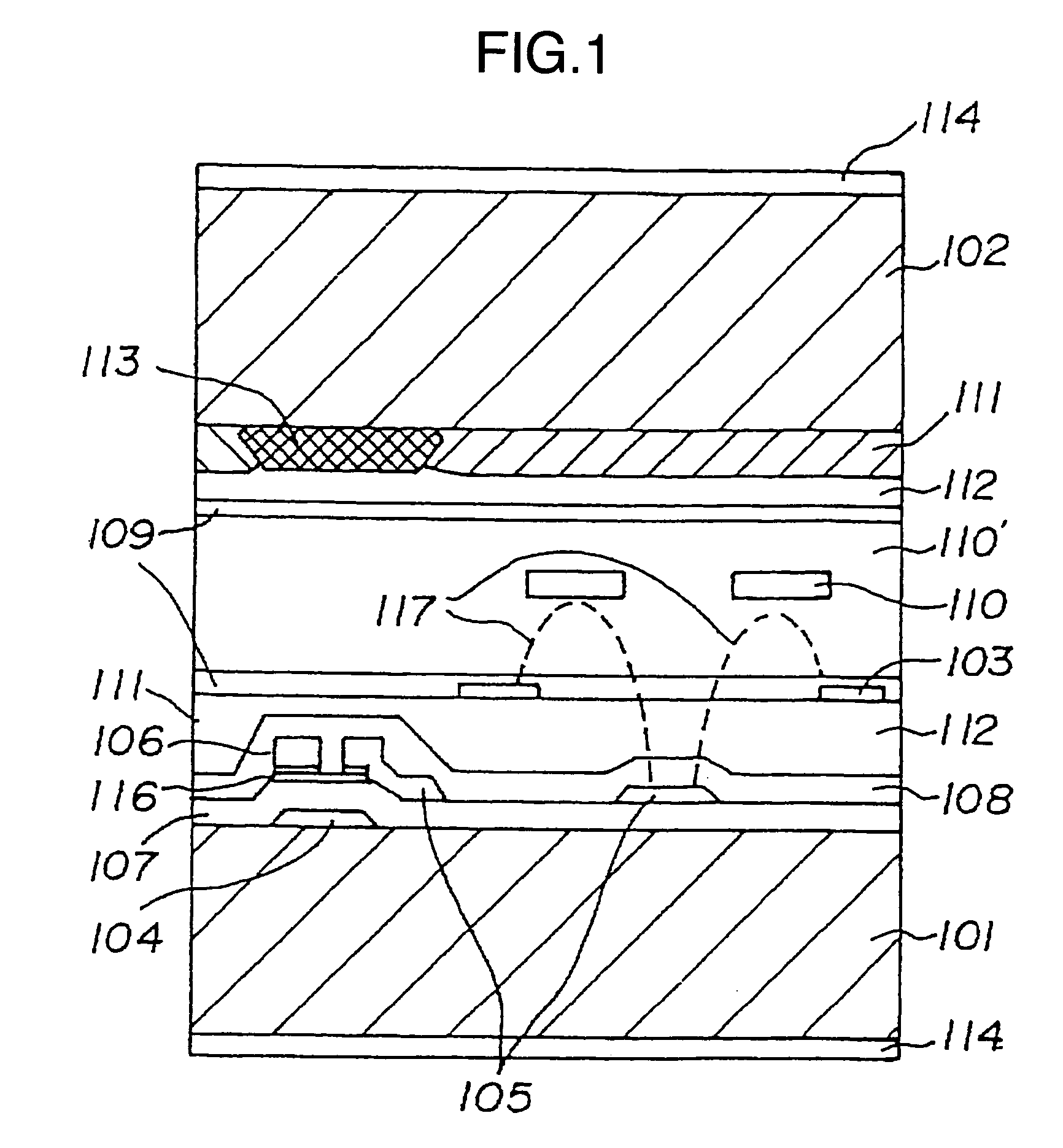
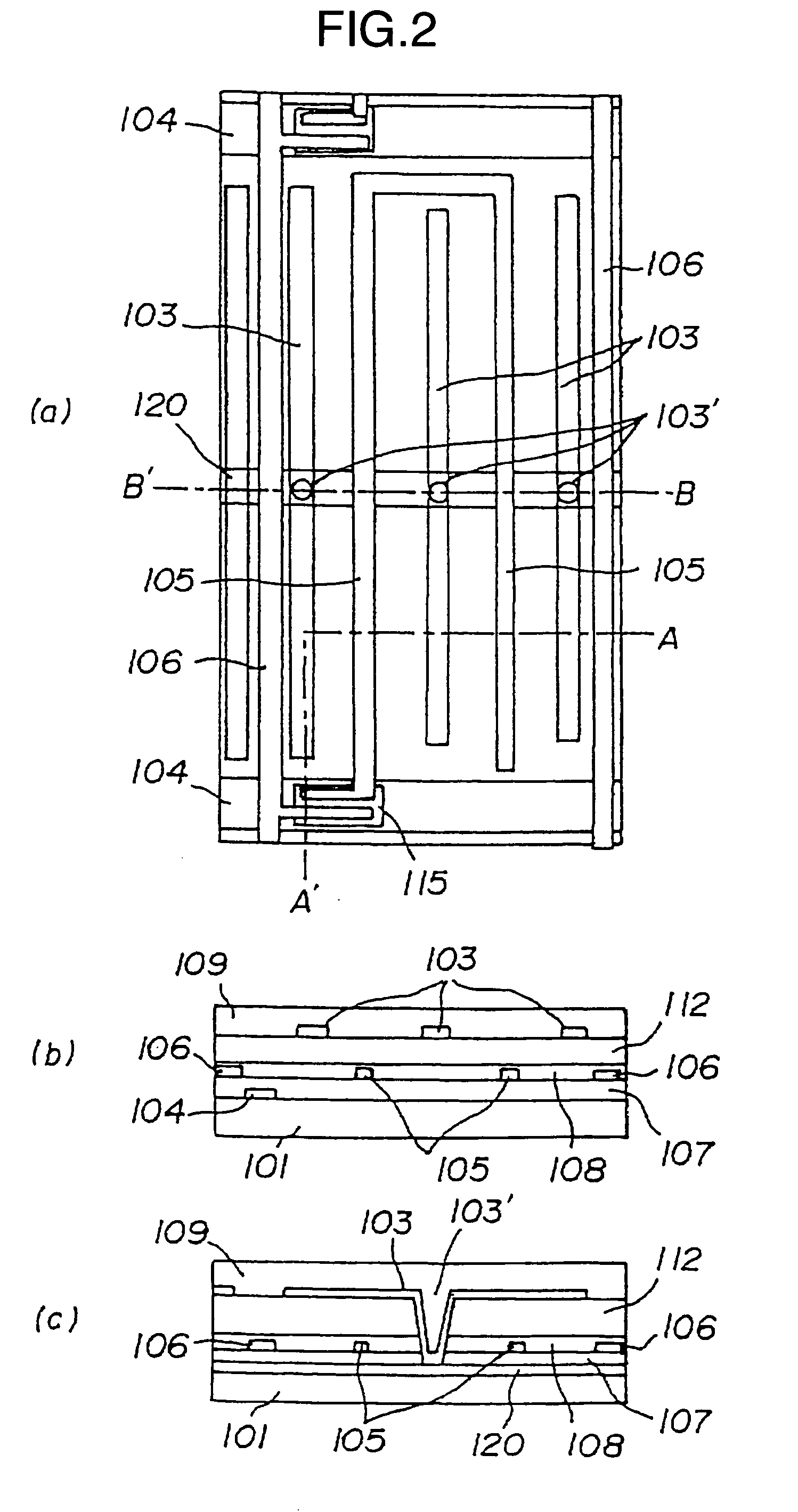
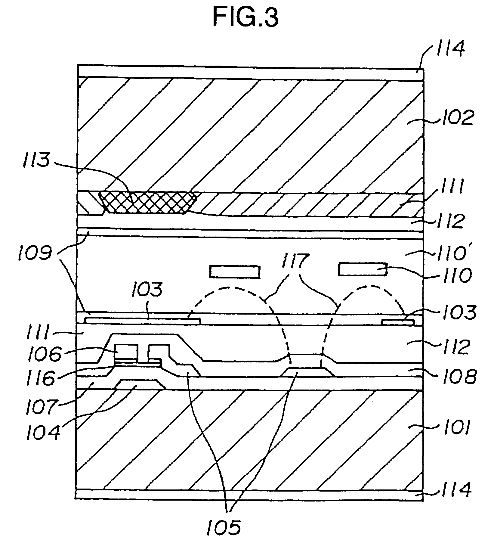
[0083] Example 1 corresponds to the liquid crystal display described in Embodiment 1 of the present invention explained above. Detailed description will hereinafter be made for Example 1 of the present invention with reference to FIGS. 1 and 2.

[0084] In producing the liquid crystal display which is Example 1 of the present invention, a glass substrate with a thickness of 0.7 mm and having polished surfaces is used as the glass substrate 101 constituting the active matrix substrate and the glass substrate 102 constituting the opposite substrate (color filter substrate). A thin film transistor 115 formed above the glass substrate 101 is comprised of the pixel electrode 105, the signal electrode 106, the scanning electrode 104, and the amorphous silicon 116. All of the scanning electrode 104, the common electrode wire 120, the signal electrode 106, and the pixel electrode 105 were formed by patterning a chromium film. The interval between the pixel electrode 105 and the comm...

Example

EXAMPLE 2

[0096] In the same manner as in Example 1 except the alignment control film used in Example 2, polyamic acid comprising 1,3-dimethyl-1,2,3,4-cyclobutanetetracarboxylic acid dianhydride shown in a formula [35] as acid dianhydride and m-phenylenediamine shown in a formula [36] as a diamine compound was formed through printing on the substrate surface and subjected to firing at 230° C. for 30 minutes for imidation, thereby depositing the film with a thickness of approximately 50 nm. Then, while the substrate was heated to 200° C. by a hot plate, the surface was subjected to photo-alignment processing through light irradiation with polarized UV of krF excimer laser with a wavelength of 248 nm and nitrogen laser with a wavelength of 337 nm.

[0097] Thereafter, a nematic liquid crystal composition A was filled in the same manner as in Example 1. Annealing was then performed at 100° C. for 10 minutes. Thus, favorable liquid crystal alignment was provided in a direction substantia...

Example

COMPARATIVE EXAMPLE 1

[0100] As a Comparative Example 1 for explaining the effect of Example 2, a liquid crystal display panel was formed in the same manner as in Example 1 except the alignment control film by using polyamic acid varnish consisting of pyromellitic acid dianhydride shown in a formula [37] as acid dianhydride and p-phenylenediamine shown in a formula [38] as a diamine compound.

[0101] When the display quality thereof was evaluated in the same manner as in Example 1, a wide viewing angle substantially equivalent to that of the liquid crystal display of Example 1 was observed, although the display with a contrast ratio of lower than 100:1 over the entire screen was observed. Similarly to Example 1, the image persistence and after-image relaxation time of the liquid crystal display were quantitatively evaluated, and the after-image relaxation time was found approximately seven minutes in a range of operating temperatures from 0 to 50° C. Also, in the visual image qualit...


PUM

PropertyMeasurementUnit
Temperatureaaaaaaaaaa
Fractionaaaaaaaaaa

Abstract

A liquid crystal display is provided which is capable of reducing the occurrence of defective display due to variations in the initial alignment direction of a liquid crystal alignment control film in a liquid crystal display of an IPS scheme, realizing the stable liquid crystal alignment, providing excellent mass productivity, and having high image quality with a higher contrast ratio. The liquid crystal display has a liquid crystal layer disposed between a pair of substrates, at least one of the substrates being transparent, and an alignment control film formed between the liquid crystal layer and the substrate. At least one of the alignment control films comprises photoreactive polyimide and/or polyamic acid provided with an alignment control ability by irradiation of substantially linearly polarized light.

Description

TECHNICAL FIELD [0001] The present invention relates to a liquid crystal display of a so-called IPS (In-Plane Switching) scheme in which an electric field substantially in parallel with a substrate is applied to a liquid crystal layer for operation, and to a production process thereof. BACKGROUND ART [0002] In general, display of a liquid crystal display is realized by applying an electric field to liquid crystal molecules in a liquid crystal layer sandwiched between a pair of substrates to change the alignment direction of the liquid crystal molecules and utilizing the resulting change in the optical property of the liquid crystal layer. Conventionally, a liquid crystal display of a so-called active drive type having a switching device such as a thin-film transistor for each pixel is represented by a TN (Twisted Nematic) display scheme in which an electrode is provided for each of a pair of substrates sandwiching a liquid crystal layer between them, the direction of an electric fie...

Claims


Application Information

Patent Timeline
IPC IPC(8): G02F1/1337G02F1/1343C08G73/10
CPCG02F1/133723G02F1/133788G02F1/134363C09D179/08C09K19/542Y10T428/1018Y10T428/1005Y10T428/1023Y10T428/1027Y10T428/10Y10T428/1036C09K2019/548C09K2323/0271C09K2323/025C09K2323/027C09K2323/02C09K2323/03C09K2323/00G02F1/1337C08G73/10C09K19/56G02F2201/121G02F2201/123G02F2202/08
Inventor TOMIOKA, YASUSHIABE, HIDETOSHIKONDO, KATSUMI
Owner NISSAN CHEM IND LTD
Why Eureka
Try Eureka