Dielectric thin film, thin film capacitor element, and method for manufacturing thin film capacitor element

a technology of capacitor elements and dielectric thin films, which is applied in the direction of fixed capacitors, thin/thick film capacitors, fixed capacitor details, etc., can solve the problems of difficult to achieve the high dielectric constant and leakage characteristics of dielectrics, adversely affecting productivity, and difficult to obtain the targeted temperature characteristics in these layers. , to achieve the effect of good dielectric constant temperature characteristics, high dielectric constant, and easy manufacturing

Inactive Publication Date: 2006-04-06
TDK CORPARATION
View PDF3 Cites 7 Cited by
  • Summary
  • Abstract
  • Description
  • Claims
  • Application Information

AI Technical Summary

Benefits of technology

[0014] In view of this, it is an object of the present invention to provide a dielectric thin film that is a BST-based dielectric thin film, has good dielectric constant temperature characteristics (the absolute value of the temperature coefficient is extremely small), and is easy to manufacture. It is another object of the present inventions to provide a dielectric thin film with a high dielectric constant and good leak characteristics.
[0015] As a result of diligent study into BST thin film materials, the inventors discovered that while it is generally held that BST bulk materials have a high temperature coefficient as mentioned above, when a thin film of 500 nm or less was produced in the course of trial and error, the electrical characteristics of this film did not necessarily match the tendency of bulk materials. Specifically, the inventors arrived at the present invention upon discovering that even with a BST material, a dielectric thin film that has good temperature characteristics, a high dielectric constant and a low leakage current density can be obtained by controlling the composition to a specific range, and controlling the ratio of the diffraction line peak intensity of the (100) plane and the (110) plane to a specific range.

Problems solved by technology

The inventions of Japanese Laid-Open Patent Application H9-293629 and Japanese Laid-Open Patent Application 2002-75783, meanwhile, at least two dielectric thin film layers to be formed, and the problem with increasing the number of thin film formation steps is that it adversely affects productivity.
Furthermore, it is difficult to achieve the dielectric high dielectric constant and leak characteristics in addition to good temperature characteristics.
Moreover, forming the various dielectric layers by sol-gel method is given as an example in Japanese Laid-pen Patent Application H9-293629, but the heat treatment performed for crystallization causes inter-diffusion at the interface between the two layers, and it is difficult to obtain the targeted temperature characteristics in these layers.

Method used


Image

  • Dielectric thin film, thin film capacitor element, and method for manufacturing thin film capacitor element
  • Dielectric thin film, thin film capacitor element, and method for manufacturing thin film capacitor element

Examples


examples

[0037] The present invention will now be described in further detail through examples, but the present invention is not to the following examples.

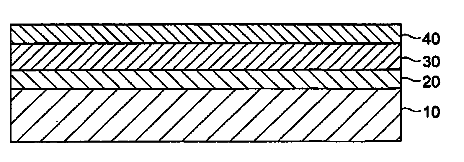
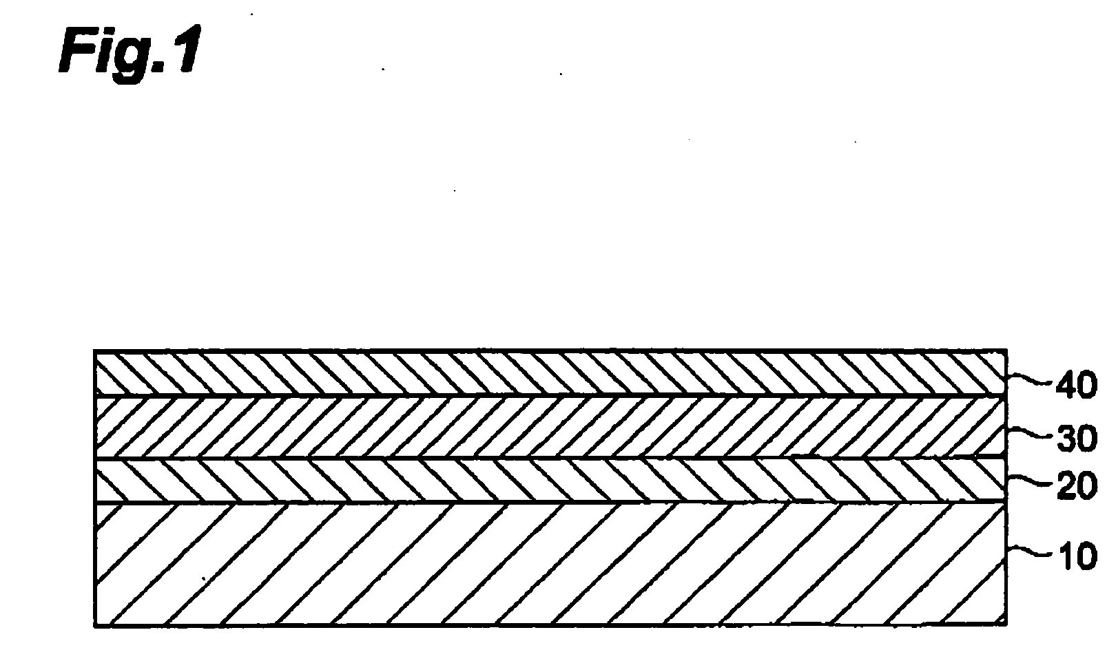
[0038] A 20 nm TiO2 film was formed as an adhesion layer over a silicon substrate on whose surface a thermal oxidation film (SiO2) had been formed. A lower electrode layer was then formed by sputtering over the adhesion layer. The electrode material was platinum, and the thickness was 100 to 150 nm. A dielectric thin film with the composition shown in Table 1 was then formed by sputtering with a BST target of a specific composition over the lower electrode layer. This film was formed in a mixed gas atmosphere containing argon gas and 10 to 25 vol % oxygen gas, at a substrate temperature of 550° C., a film formation pressure of 0.3 to 4 Pa, an it power of 1.3 to 1.8 W / cm2, and a film formation rate of 4 to 5 nm / min. The thickness of the dielectric thin film was from 100 to 140 nm.

[0039] Thin films of various compositions were then anneale...


PUM

PropertyMeasurementUnit
Temperatureaaaaaaaaaa

Abstract

The present invention provides a dielectric thin film whose composition is expressed by the formula (Ba1-xSrx)yTiO3 (0.18≦x≦0.45, 0.96≦y≦1.04), and whose peak intensity ratio I(100)I(110) is from 0.02 to 2.0 when I(100) is the peak intensity of the diffraction line of the (100) plane, and I(110) is the peak intensity of the diffraction line of the (110) plane in an X-ray diffraction chart of the dielectric thin film.

Description

BACKGROUND OF THE INVENTION [0001] 1. Field of the Invention [0002] The present invention relates to a dielectric thin film and a thin film capacitor element that have a high dielectric constant, good temperature characteristics of the dielectric constant, and good leak characteristics, and a method for manufacturing the thin film capacitor element. [0003] 2. Description of the Related Art [0004] As electronic devices have rapidly become smaller and higher in performance in recent years, the electronic circuitry used in these devices has increased in density and integration, and there has been a need for even smaller capacitor elements and other such circuit elements that are essential to various electronic circuits. For instance, thin film capacitors that make use of dielectric thin films have come to be widely used in integrated circuits with active elements such as transistors. [0005] SiO2, Si3N4, and other such materials have been used in the past for thin film capacitors, but f...

Claims


Application Information

Patent Timeline
IPC IPC(8): H01G4/20
CPCH01G4/1227H01G4/33H01L21/31691H01L27/016H01L28/55H01L28/65H01L21/02266H01L21/02197
Inventor UCHIDA, KIYOSHIHORINO, KENJISAITA, HITOSHI
Owner TDK CORPARATION
Why Eureka
Try Eureka