Annealed wafer and anneald wafer manufacturing method

Active Publication Date: 2006-04-13
SHIN-ETSU HANDOTAI CO LTD
View PDF7 Cites 27 Cited by
  • Summary
  • Abstract
  • Description
  • Claims
  • Application Information

AI Technical Summary

Benefits of technology

[0030] With the foregoing problem of the prior art in view, it is an object of the present invention to provide an annealed wafer which has an excellent oxide film dielectric breakdown characteristic in a wafer surface layer serving as a

Problems solved by technology

In particular, there exist defects due to single crystal growth called grown-in defects such as FPD, LSTD, and COP, which deteriorate an oxide film dielectric breakdown characteristic and the characteristics of a device.
However, it has become clear that a very large number of oxide film defects may be generated even in a single crystal where an N region spreads on the entire surface, an OSF ring is not generated when performing thermal oxidation treatment, and FPD and L/D are not present on the entire surface.
This is a cause of deteriorating electric characteristics such as an oxide film dielectric breakdown characteristic.
It is known that defects such as COP are present at a portion where the oxide film is easily deteriorated.
Therefore, the oxide precipitates which are present before loading the wafer into the device fabrication processes are extremely small, and do not have the IG capability.
On the other hand, in recent device fabrication processes, with an increase in diameter of a wafer to be used, there progresses loweri

Method used


Image

  • Annealed wafer and anneald wafer manufacturing method
  • Annealed wafer and anneald wafer manufacturing method
  • Annealed wafer and anneald wafer manufacturing method

Examples


example 1

[0119] A silicon single crystal was pulled by the Czochralski method in a region of (Nv-Dn)+Ni in FIG. 10 (JP A 2002-201093) under controlling a growth rate between a first growth rate at a boundary where a defective region (Dn) left after annihilation of an OSF ring and detectable by a Cu deposition method is annihilated when the growth rate of pulling a silicon single crystal was gradually reduced, and a second rate at a boundary (a boundary between an N region and an I region) where an interstitial dislocation loop is generated when the growth rate is further gradually reduced, so that there was prepared a mirror-polished silicon wafer manufactured from a silicon single crystal pulled in a condition that the generation of voids was suppressed.

[0120] In the growth of the crystal, nitrogen was not added. The wafer has a diameter of 8 inches, a crystal orientation of , and a resistivity of about 10 Ω·cm (boron doped). Wafers of two types having different oxygen concentrations were ...

example 2

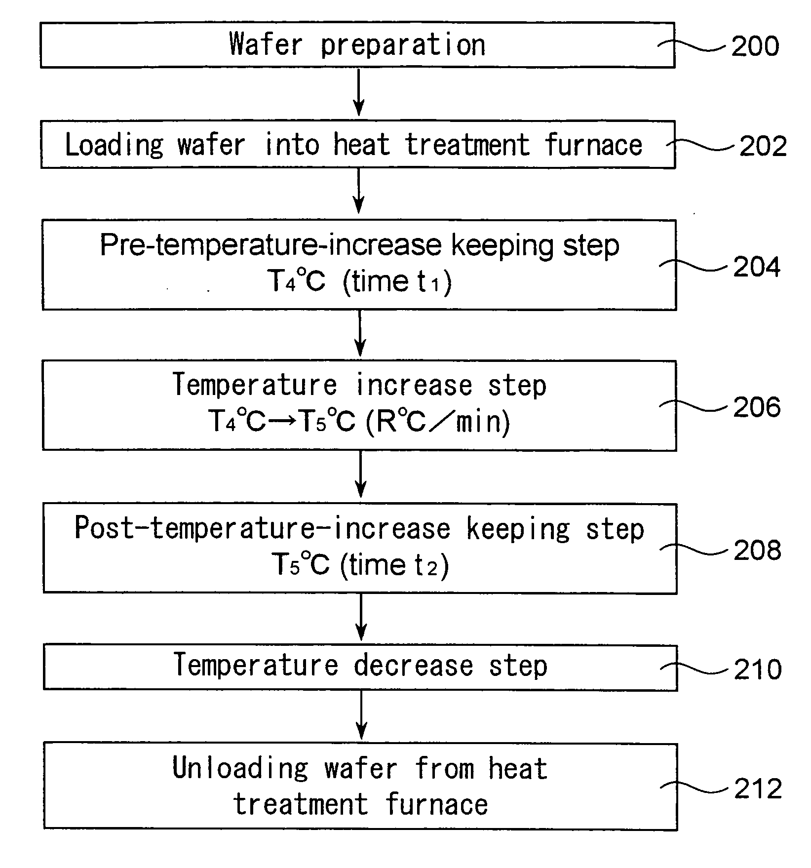
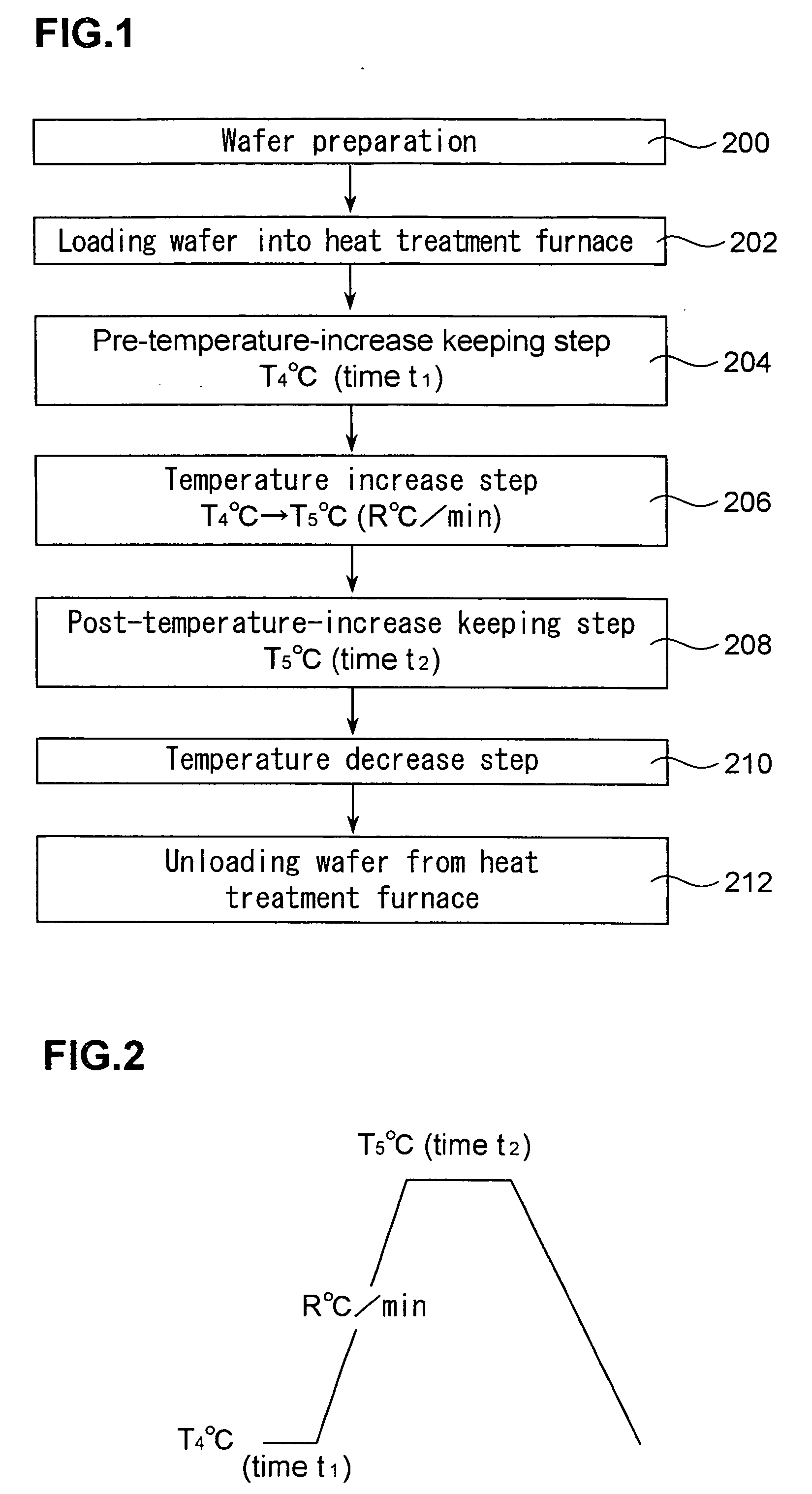
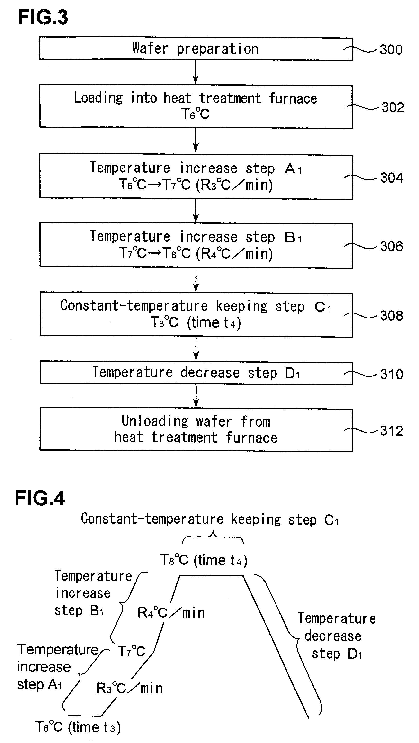
[0125] The silicon mirror-polished wafers manufactured in the same conditions as those in Example 1 were subjected to the following heat treatment in an argon atmosphere. That is, the wafers were kept at 700° C. for 1 hour, the temperature was increased to 900° C. at a rate of 3° C. / min, and increased from 900° C. to 1200° C. at a rate of 5° C. / min, and the wafers were kept at 1200° C. for 1 hour. After the keeping, the inside temperature of the heat treatment furnace was decreased to 700° C. at a rate of 3° C. / min, and the wafers were unloaded from the heat treatment furnace.

[0126] On the wafers (annealed wafers) subjected to the heat treatment, TZDB good chip yields and densities of the oxide precipitates were measured under the same conditions as those in Example 1. As a result, in all cases of the oxygen concentrations, as in Example 1, the good chip yields in the regions having a depth of at least up to 5 μm were almost 100%, and those in the regions having a depth of up to on...


PUM


Abstract

The present invention provides an annealed wafer which has a wafer surface layer serving as a device fabricating region and having an excellent oxide film dielectric breakdown characteristic, and a wafer bulk layer in which oxide precipitates are present at a high density at the stage before the wafer is loaded into the device fabrication processes to give an excellent IG capability, and a method for manufacturing the annealed wafer. The present invention is directed to an annealed wafer obtained by performing heat treatment on a silicon wafer manufactured from a silicon single crystal grown by the Czochralski method, wherein a good chip yield of an oxide film dielectric breakdown characteristic in a region having at least a depth of up to 5 μm from a wafer surface is 95% or more, and a density of oxide precipitates detectable in the wafer bulk and each having a size not smaller than a size showing a gettering capability is not less than 1×10⁹/cm3.

Description

TECHNICAL FIELD [0001] The present invention relates to an annealed wafer having a wafer surface layer with an excellent oxide film dielectric breakdown characteristic and a wafer bulk layer with an excellent gettering capability, and a method for manufacturing the annealed wafer. BACKGROUND ART [0002] In recent years, with miniaturization of a device in consequence of an increase in an integration level of a semiconductor circuit, there have risen quality requirements for a silicon single crystal serving as a substrate of the semiconductor circuit and grown by a Czochralski method (hereinafter referred to, for brevity, as the “CZ method”). In particular, there exist defects due to single crystal growth called grown-in defects such as FPD, LSTD, and COP, which deteriorate an oxide film dielectric breakdown characteristic and the characteristics of a device. A decrease in the density and sizes of the defects is regarded as important. [0003] In explanation of these defects, first ther...

Claims


Application Information

Patent Timeline
IPC IPC(8): C30B23/00C30B25/00C30B28/14C30B28/12C30B29/06C30B33/00C30B33/02H01L21/322
CPCC30B29/06C30B33/02H01L21/3225H01L21/322
Inventor TAKENO, HIROSHISAKURADA, MASAHIROKOBAYASHI, TAKESHI
Owner SHIN-ETSU HANDOTAI CO LTD
Why Eureka
Try Eureka