Semiconductor integrated circuit

a technology of integrated circuits and semiconductors, applied in the field of protection circuits, can solve problems such as leakage of clamp mos transistors, waste of power consumption, unstable input of the gate of the clamp mos transistor, etc., and achieve the effects of reducing clamp voltage, increasing clamping operation speed, and high resistan

Active Publication Date: 2006-04-27
RENESAS ELECTRONICS CORP
View PDF10 Cites 20 Cited by
  • Summary
  • Abstract
  • Description
  • Claims
  • Application Information

AI Technical Summary

Benefits of technology

[0022] By short-circuiting the gate of the clamp MOS transistor and the ground line with high resistance, the clamping operation of the protection circuit can be prevented from being erroneously performed by power source noise.
[0023] By biasing the substrate region of the clamp MOS transistor on the basis of the voltage at the connection node of the resistor and the capacitor connected in series between the power source line and the ground line, the invention can contribute to decrease the clamp voltage and increase the speed of the clamping operation.
[0024] By employing the thyristor and the MOS transistor in parallel in the final stage of the clamp circuit, the speed of the clamping for high voltage fluctuations in the semiconductor integrated circuit which is operated with low voltage can be increased.

Problems solved by technology

First, it was clarified by the inventors herein that an output of the CMOS inverter excessively reacts to power source noise, an input of the gate of the clamp MOS transistor becomes unstable, and there is the possibility that a leak occurs in the clamp MOS transistor.
Such a leak causes waste power consumption.

Method used


Image

  • Semiconductor integrated circuit
  • Semiconductor integrated circuit
  • Semiconductor integrated circuit

Examples


Embodiment Construction

Gate Bias and Well Bias for Clamp MOS Transistor

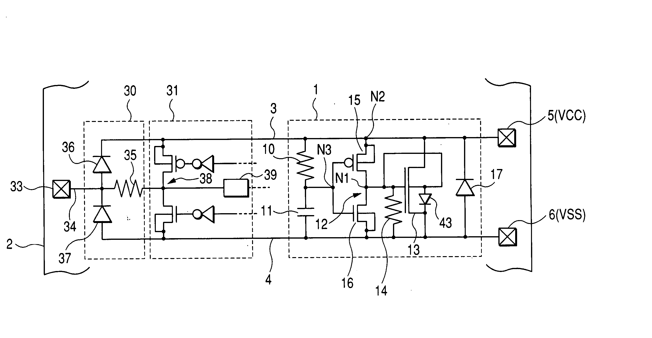
[0037]FIG. 1 shows an example of a protection circuit of a semiconductor integrated circuit according to the present invention. A protection circuit 1 shown in the diagram is mounted on a semiconductor integrated circuit 2 such as a logic LSI, a memory LSI, or the like of a microcomputer or the like formed by the CMOS integrated circuit manufacturing technique on a single semiconductor substrate such as a single crystal silicon. The protection circuit 1 is disposed between a power source line 3 as a first line and a ground line 4 as a second line and, in response to an application of a high voltage by ESD or the like, functions to make the high voltage escape from one end to the other end. In the embodiment, the power source line 3 serves as a power source main line connected to an external power source pad 5, and the ground line 4 serves as a ground main line connected to an external ground pad 6. A power source voltage VCC is suppl...


PUM


Abstract

The present invention is provided to suppress occurrence of an erroneous operation in a protection circuit due to a relatively small power source fluctuation such as a power source noise. The protection circuit has a first resistor and a capacitor connected in series between a power source line and a ground line, an inverter whose input is connected between the first resistor and the capacitor, and a MOS transistor whose gate electrode receives an output of the inverter and whose drain electrode and source electrode are connected to the power source line and the ground line. When a high voltage fluctuation occurs in the power source line, a level change at a connection point between the first resistor and the capacitor is delayed according to a time constant. By the delay, the MOS transistor that receives an output of the inverter is temporarily turned on and discharges a high voltage to the ground line. Since an output of the inverter is pulled down to the ground line via a second resistor, even if an output of the inverter fluctuates undesirably, fluctuations in a gate input of the MOS transistor are suppressed.

Description

CROSS-REFERENCE TO RELATED APPLICATION [0001] The present application claims priority from Japanese patent application No. 2004-309960 filed on Oct. 25, 2004, the content of which is hereby incorporated by reference into this application. BACKGROUND OF THE INVENTION [0002] The present invention relates to a protection circuit for suppressing destruction of an internal circuit by fluctuations in high voltage due to electrostatic discharge (ESD) for an input terminal and a power source terminal in a semiconductor integrated circuit. [0003] Japanese Patent Laid-open No. 2004-14929 (FIG. 1, paragraph 0060) discloses a protection circuit against the ESD having a configuration including a resistive element and a capacitive element connected in series between a power source line and a ground line, a CMOS inverter whose input is connected between the resistive element and the capacitive element, and an n-channel type clamp MOS transistor whose gate electrode receives an output of the CMOS i...

Claims


Application Information

Patent Timeline
Patent Type & Authority Applications(United States)
IPC IPC(8): H02H9/00
CPCH01L27/0251H01L2924/0002H01L2924/00H01L21/82H01L21/77
Inventor ISHIZUKA, HIROYASUTANAKA, KAZUO
Owner RENESAS ELECTRONICS CORP
Why Eureka
Try Eureka