Semiconductor device having a stacked capacitor

a technology of stacked capacitors and semiconductor devices, which is applied in the direction of semiconductor devices, capacitors, electrical equipment, etc., can solve the problems of tantalum oxide problems, difficult to use hsg structures, and difficult to meet the requirements of stacked capacitors, etc., to achieve the effect of reducing leakage current, reducing thickness, and reducing the thickness

Inactive Publication Date: 2006-05-18
ELPIDA MEMORY INC
View PDF4 Cites 20 Cited by
  • Summary
  • Abstract
  • Description
  • Claims
  • Application Information

AI Technical Summary

Benefits of technology

[0008] The present inventor noticed aluminum oxide in the study for achieving a thin capacitor insulation film in the stacked capacitor. Use of the aluminum oxide obviates a heat treatment for achieving a lower leakage current and thus provides a smaller thickness as small as 1 nm or smaller for the low-dielectric-constant film, which is generally formed on a silicon surface by oxidization thereof. This allows the capacitor insulation film to have a smaller thickness by 2.5 nm or more compared to the case of using the tantalum oxide as the capacitor insulation film.

Problems solved by technology

In such a development of finer design rule, a stacked capacitor used in each memory cell of the DRAM device also has reduced dimensions, which makes it difficult for the stacked capacitor to have a required capacitance.
However, in the F90-rule DRAM device, it is difficult to use the HSG structure due to the finer design rule, wherein the polysilicon bottom electrode is not allowed to have the HSG structure because of the difficulty in formation of the hemispherical grains on the surface thereof.
However, the tantalum oxide has a problem of occurring of silicon oxynitride film having a lower dielectric constant, after the silicon electrode reacts with an adjacent tantalum oxide film in a heat treatment conducted for reducing a leakage current in the capacitor.

Method used


Image

  • Semiconductor device having a stacked capacitor
  • Semiconductor device having a stacked capacitor
  • Semiconductor device having a stacked capacitor

Examples


first embodiment

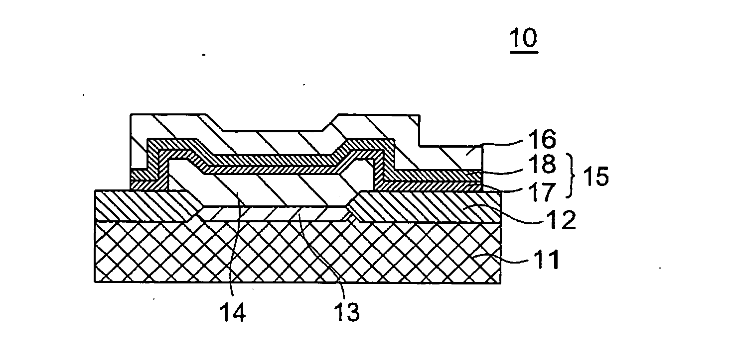
[0091] Now, the embodiments of the present invention are specifically described with reference to accompanying drawings. FIG. 20 shows a layer structure of a capacitor in a semiconductor device according to the present invention. The semiconductor device 10 includes a silicon substrate 11, a LOCOS film 12 formed on the silicon substrate 11 for isolation of element regions, a titanium silicide film 13 formed on the element region of the silicon substrate 11, and a layered structure of a capacitor formed on the titanium silicide film 13. The capacitor includes a bottom electrode 14 made of titanium nitride formed on the titanium silicide film 13, a capacitor insulation film 15 having a two-layer structure, and a top electrode 16 made of titanium nitride. Other insulator films and interconnect patterns are omitted for depiction in the drawing.

[0092] The titanium silicide film 13 reduces the contact resistance between the bottom electrode 14 and the silicon substrate 11. The capacitor i...

second embodiment

[0110] A semiconductor device of a modification from the second embodiment shown in FIG. 24 is such that the hafnium oxide 22 sandwiched between the aluminum oxide films 21 and 23 in FIG. 24 has a polycrystalline structure. The term polycrystalline structure used herein means that every measurable area has an exclusive crystalline structure and does not assume an amorphous state. The polycrystalline structure can be identified using an X-ray diffraction technique or transmission electron microscope.

[0111] In manufacture of the semiconductor device of the modification, formation of the bottom electrode 14 is followed by consecutively depositing 2-nm-thick aluminum oxide 21, 3-nm-thick hafnium oxide 22 and 2-nm-thick aluminum oxide 23, all of them in an amorphous state. Thereafter, in a nitrogen atmosphere, a heat treatment is performed at a temperature of 700 degrees C. for 3 minutes. Since the crystallizing temperature for the hafnium oxide 22 is 550 degrees C., the hafnium oxide 22...

third embodiment

[0116]FIG. 29 shows a semiconductor device according to the present invention. The semiconductor device 100 configures a DRAM device including a memory cell area 100A wherein a plurality of memory cells are arranged in a matrix on a p-type silicon substrate 101. The silicon substrate 101 includes an n-well 102 in the surface region thereof, and a first p-well 103 in the surface region of the n-well 102. The DRAM device 100 also includes a peripheral circuit area 100B, wherein the silicon substrate 101 includes a second p-well 104 in the surface region thereof, the second p-well 104 being isolated from the first p-well 103 by an element isolation area 105.

[0117] Switching transistors 106, 107 each configuring a memory cell are formed on the first p-well 103. Transistor 106 includes a drain 108, a source 109, and a gate electrode 111 formed on the silicon substrate 101 with an intervention of a gate insulation film 110. Transistor 107 includes the source 109 provided in common with tr...


PUM

PropertyMeasurementUnit
thicknessaaaaaaaaaa
thicknessaaaaaaaaaa
thicknessesaaaaaaaaaa

Abstract

A stacked capacitor in a memory cell has a bottom electrode made of a metal or metal compound, a capacitor insulation film and a top electrode made of a metal or a metal compound. The capacitor insulation film includes an aluminum oxide film having a thickness of 2 to 4 nm and in contact with the bottom electrode, and an overlying hafnium oxide film having a thickness of 3 to 6 nm. The stacked capacitor has a higher resistance against a biased temperature test.

Description

BACKGROUND OF THE INVENTION [0001] (a) Field of the Invention [0002] The present invention relates to a semiconductor device having a stacked capacitor and, more particularly, to a technique for reducing dimensions of a semiconductor device having a stacked capacitor while assuring a higher capacitance of the stacked capacitor. The present invention also relates to a method for manufacturing such a semiconductor device. [0003] (b) Description of the Related Art [0004] Semiconductor devices have been developed to reduce the dimensions and increase the scale and functions thereof. In particular, DRAM devices now on the market have a capacity of giga-bit order with a reduced design rule of 110 nm (F110-rule), and next-generation DRAM devices will have such an order of capacity with a further reduced design rule of 90 nm (F90-rule). In such a development of finer design rule, a stacked capacitor used in each memory cell of the DRAM device also has reduced dimensions, which makes it diff...

Claims


Application Information

Patent Timeline
Patent Type & Authority Applications(United States)
IPC IPC(8): H01L29/00
CPCH01L21/02178H01L21/02181H01L21/022H01L21/0228H01L21/3142H01L21/3162H01L21/31645H01L28/40
Inventor IIJIMA, SHINPEI
Owner ELPIDA MEMORY INC
Why Eureka
Try Eureka