Magnetic head and magnetic recording/reproducing system
a magnetic recording/recording and head technology, applied in the field of magnetic head, can solve the problems of low yield, difficulty in reducing the shield to shield distance to 70 nm or less, and still have problems to be solved, and achieve the effect of high yield and high outpu
- Summary
- Abstract
- Description
- Claims
- Application Information
AI Technical Summary
Benefits of technology
Problems solved by technology
Method used
Image
Examples
embodiment 1
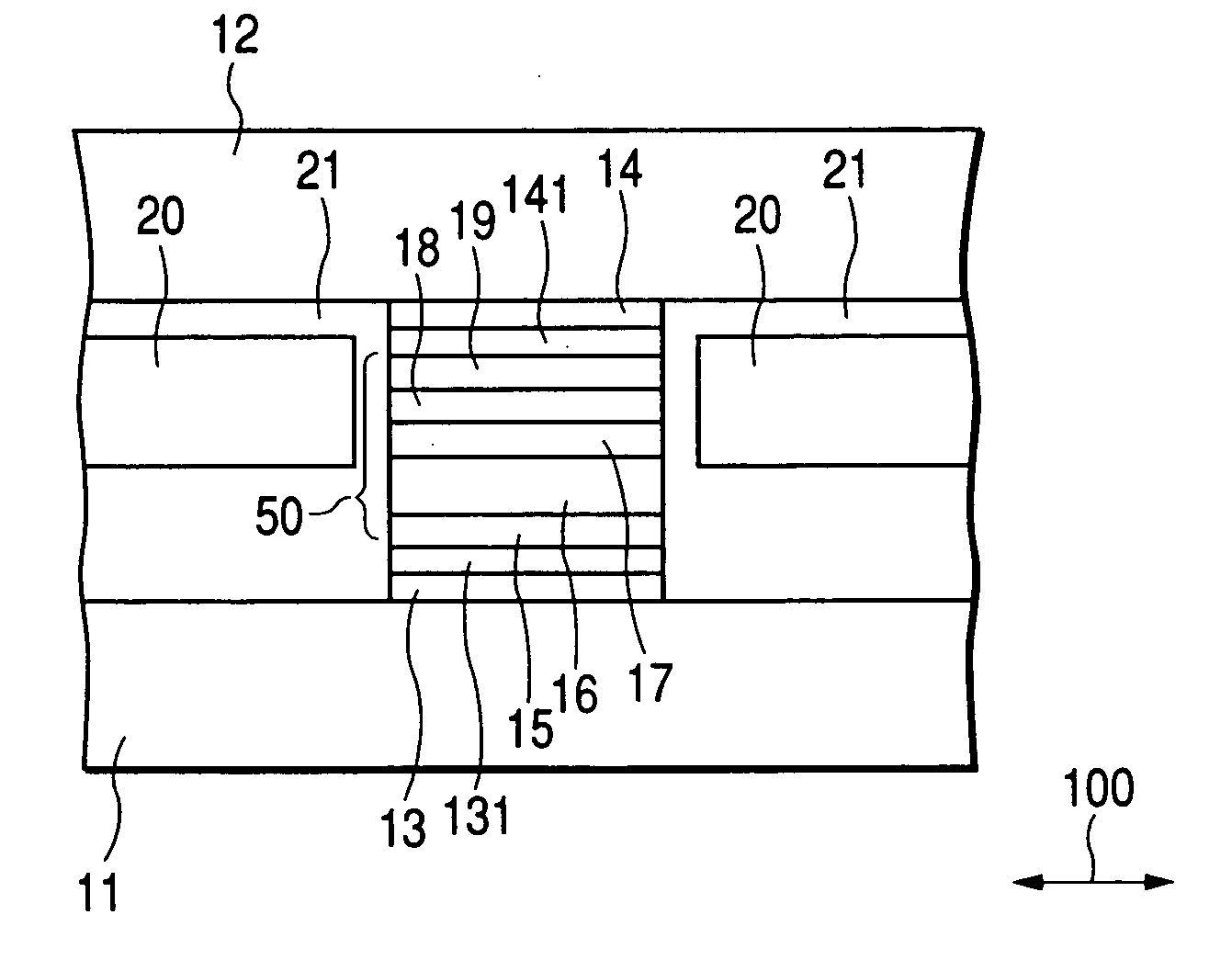
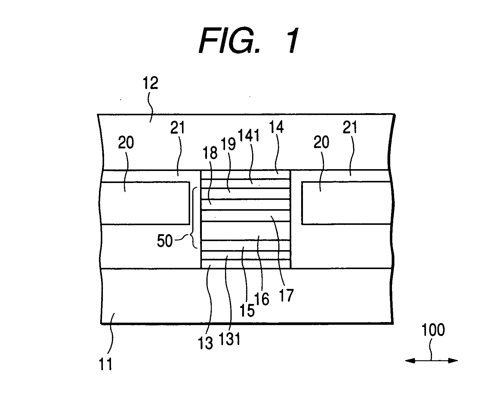
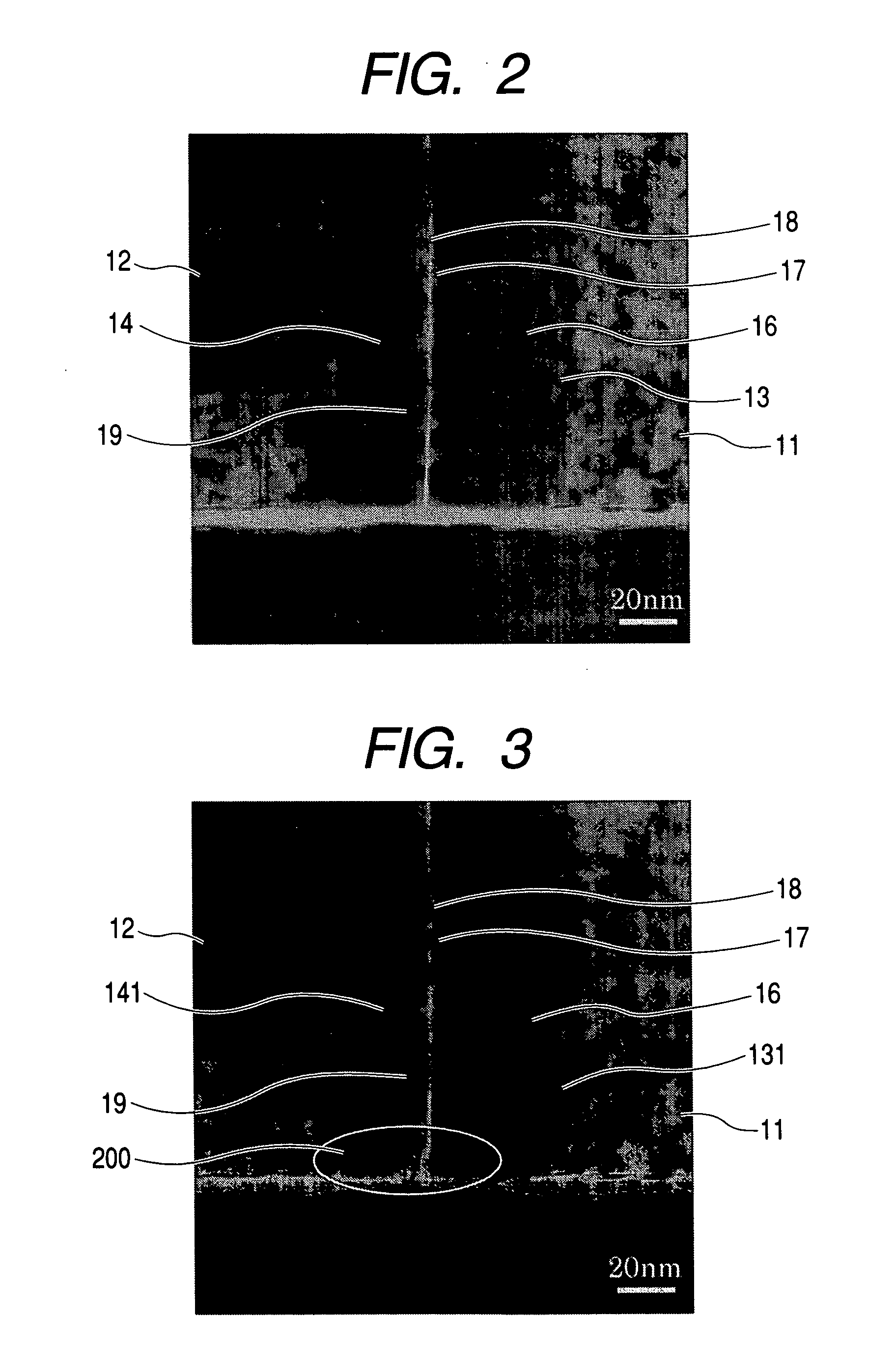
[0049]FIG. 1 shows the structure of the air bearing surface of the magnetoresistive head of the present invention. A lower shield layer 11 made from a Ni—Fe alloy and having a predetermined shape is formed on an alumina-titanium carbide substrate coated with an insulator such as alumina, and a lower first deformation prevention layer 13 made from Mo, a lower gap layer 131 made from Ta, a CPP magnetoresistive film 50, an upper gap layer 141 made from Cu and an upper first deformation prevention layer 14 made from Mo are formed on the lower shield layer 11.
[0050] The CPP magnetoresistive film 50 consists of a seed layer 15 made from a metal for controlling the orientation of a laminate film formed thereon, for example, 81 at. % Ni-19 at. % Fe, an antiferromagnetic layer 16 made from 52 at. % of Pt and 48 at. % of Mn, a second ferromagnetic layer 17 made from 75 at. % of Co and 25 at. % of Fe, a tunnel barrier layer 18 made from aluminum oxide and a first ferromagnetic layer 19 made f...
embodiment 2
[0073] In Embodiment 1, the lower first deformation prevention layer 13 and the upper first deformation prevention layer 14 have substantially the same width in the track direction as the CPP magnetoresistive film 50. In this embodiment shown in FIG. 5, they have a larger width than the CPP magnetoresistive film 50. The lower first deformation prevention layer 13 can be made as wide as the lower shield layer 11 and the upper first deformation prevention layer 14 can be made as wide as the upper shield layer 12.
[0074] One example of the production process is as follows. After the lower shield layer 11 is formed, the lower first deformation prevention layer 13 is formed and patterned to a desired shape by a dry etching method or ion milling method. The CPP magnetoresistive film 50 is formed, a lift-off mask is formed at a position which becomes a magnetic sensing portion, and the upper gap layer and the CPP magnetoresistive film excluding the magnetic sensing portion are etched by th...
embodiment 3
[0076] In the structure of Embodiment 2 (FIG. 5), in order to reduce contact resistance between the lower first deformation prevention layer 13 and the shield layer 15 and between the first ferromagnetic layer 19 and the upper first deformation prevention layer 14, the surfaces of the lower first deformation prevention layer 13 and the first ferromagnetic layer 19 must be cleaned by sputter etching or the like. This cleaning varies the thickness of the lower first deformation prevention layer 13 and the thickness of the first ferromagnetic layer 19, whereby the distance between the lower shield layer and the upper shield layer (to be herein referred to as a “shield to shield distance”) changes in the former case and read sensitivity and the asymmetry of the output wavelength vary in the latter case.
[0077]FIG. 6 shows the structure capable of reducing changes in properties caused by cleaning. After the lower shield layer 11 is formed and its surface is cleaned by sputter etching or ...
PUM
| Property | Measurement | Unit |
|---|---|---|
| shear modulus | aaaaa | aaaaa |
| magnetization | aaaaa | aaaaa |
| height | aaaaa | aaaaa |
Abstract
Description
Claims
Application Information


