
Quasi group III-nitride substrates and methods of mass production of the same

Inactive Publication Date: 2006-06-15
PENG HUI
View PDF2 Cites 39 Cited by
  • Summary
  • Abstract
  • Description
  • Claims
  • Application Information

AI Technical Summary

Benefits of technology

[0016] The advantages of employing Si substrates are the following: (1) large diameter: the largest diameter of a Si wafer now is 12″, which is equivalent to 36 sapphire substrates of 2″; therefore the processes of the epitaxial growth and wafer fabrication including photolithography, etching, and disposing electrodes, are significantly simplified and throughput and yield are higher; (2) the cost of a Si substrate is much lower than that of equivalent sapphire substrates; (3) the LEDs grown on a Si substrate may be easily integrated with Si based Integrated Circuit (IC) including the control circuits of LEDs; (4) The heat dissipation rate of a Si wafer is faster than that of a sapphire wafer, both conductive and isolating quasi group III-nitride substrates may be employed for growing high power vertical and lateral GaN based LEDs respectively.
[0019] (1) The primary object of the present invention is to provide large area high quality quasi group III-nitride substrates with lower dislocation and distortion density. The diameter of a quasi group III-nitride substrate is the same as that of a Si wafer employed as the original growth substrate.
[0022] (4) The fourth object of the present invention is to provide low cost methods of manufacturing large area high quality quasi group III-nitride substrates.

Problems solved by technology

Native substrates produce the best active region quality, but suffer from limited size, cost, and availability.
Foreign substrates, such as sapphire and silicon carbide (SiC), suffer the most in active region quality and limited size.
But the flip chip process is complex and costly.
However, the removing process of original growth substrates damages the quality of active region of vertical GaN based LEDs.
However, manufacturing larger area sapphire, SiC, AlN, and GaN substrates are technically difficult and costly.
The main difficulty of growing GaN based LEDs on Si wafers is attributed to the differences of the lattice constants and the thermal expansion coefficients (TEC) between the Si substrates and the GaN based epitaxial layers.
Those differences cause huge stress in GaN based epitaxial layers, and further reduce the quality of the GaN based epitaxial layers.
When a large diameter Si wafer is employed, the uniformity issue is severe.
Firstly, even a small temperature fluctuation will cause the significant difference in the composition and the growth rate, which results in a deviation from the target wavelength and intensity of emitted light.
Secondly, even for an originally flat growth substrate which is placed on an uniformly heated susceptor of a metal organic chemical vapor deposition (MOCVD), the top surface of the original growth substrate is slightly cooler than that of the bottom surface.
This, in turn, causes a loss of contact at the edges, which become progressively cooler.
When the shear stress exceeds the critical resolved shear stress, the dislocations are generated and propagate to result in slip lines.
The uniformity issue limits the size of a substrate employed.
However the so-grown quasi GaN substrates are costly, have small area, and can only be employed for lateral GaN based LEDs.

Method used


Image

  • Quasi group III-nitride substrates and methods of mass production of the same
  • Quasi group III-nitride substrates and methods of mass production of the same
  • Quasi group III-nitride substrates and methods of mass production of the same

Examples


first embodiment

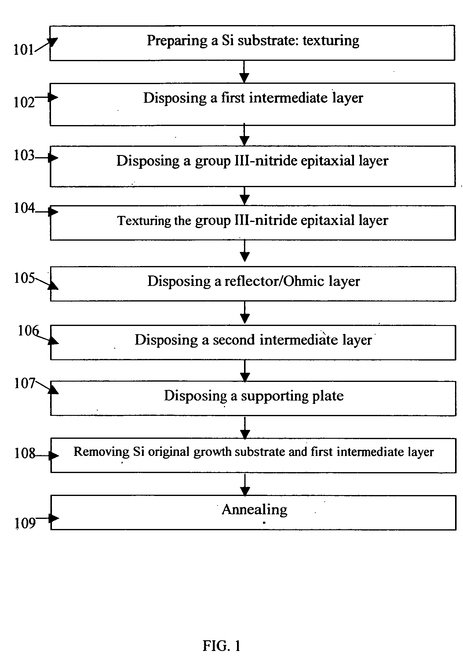
[0088] First embodiment of process 102: the first intermediate layer is an AlN layer. Disposing an AlN epitaxial layer on the surface of a Si (111) original growth substrate. The Si original growth substrate is placed in the chamber of MOCVD, at atmospheric pressure, introducing trimethylaluminum (TMA), NH.sub.3, heating up to 1000-1250 degree C., growing an AlN layer of thickness 1-500 nm with a smooth surface.

[0089] Second embodiment of process 102: the first intermediate layer is an AlN / Al layer. Disposing an Al layer of thickness of few monolayers to nanometers on the surface of a Si (111) original growth substrate for preventing the top surface of the Si original growth substrate from nitriding. Then disposing an AlN layer on the Al layer under the same condition as that of the first embodiment of process 102.

third embodiment

[0090] Third embodiment of process 102: nitriding the top surface of an Al layer. Firstly disposing an Al layer on the surface of a Si (111) original growth substrate. Introducing nitrogen source, heating up to 400-700 degree C. for 10-40 minutes, the top surface of the Al layer forms an AlN layer. Wherein the nitrogen sources comprise N.sub.2 and NH.sub.3 / H.sub.2.

fourth embodiment

[0091] Fourth embodiment of process 102: the first intermediate layer is an B.sub.xAl.sub.1-xN layer having compositional graded structure on the surface of a Si(111) original growth substrate: placing the Si original growth substrate in MOCVD, at atmosphere pressure, heat up to 1050-1150 degree C., introducing TMA, triethylboron (TEB), NH.sub.3, disposing B.sub.xAl.sub.1-xN (0≦x<1). Selecting the value of “x” such that the difference of lattice constants between the Si original growth substrate and the BAlN layer is minimized. Then gradually decreasing the flow rate of TEB, increasing the flow rate of TMA, until x=0, i.e., transfer from growing B.sub.xAl.sub.1-xN to grow AlN. The change of value of “x” may be either continuous or discrete.


PUM


Abstract

The present invention discloses the large area high quality quasi group III-nitride substrates comprising two categories: electrically conductive and isolating. The methods manufacturing the same comprise the following process steps in the order presented: disposing a first intermediate layer on a large area silicon (Si) original growth substrate, disposing a group III-nitride epitaxial layer including a n- or p-type epitaxial layer, disposing a reflector / Ohmic layer, disposing a second intermediate layer, disposing a supporting plate, removing the silicon original growth substrate and the first intermediate layer, then the group III-nitride epitaxial layer exposed. Vertical and lateral GaN based LEDs growing on electrically conductive and isolating quasi group III-nitride substrates respectively are disclosed.

Description

BACKGROUND OF THE INVENTION [0001] (1) Field of the Invention [0002] The present invention discloses large area high quality quasi group III-nitride substrates, methods of mass production of the same, and methods of manufacturing high power vertical and lateral GaN based light emitting diodes (LEDs) thereon. [0003] (2) Prior Art [0004] GaN based epitaxial materials are suitable for making optoelectronic devices or chips including GaN based light emitting diodes (LEDs). Native substrates produce the best active region quality, but suffer from limited size, cost, and availability. Foreign substrates, such as sapphire and silicon carbide (SiC), suffer the most in active region quality and limited size. [0005] High power white LEDs have potential to replace conventional light bulbs for interior lighting. But several critical issues associated with lateral GaN based LEDs need to be addressed, which include: (1) heat dissipation, (2) production cost, (3) current crowding effect, (4) outpu...

Claims


Application Information

Patent Timeline
IPC IPC(8): H01L33/00H01L21/00H01L33/40
CPCC30B29/403H01L21/0237H01L21/02381H01L21/02458H01L21/02491H01L21/02502H01L21/0251H01L21/0254H01L33/007H01L33/0079H01L33/405H01L33/0093
Inventor PENG, HUI
Owner PENG HUI
Learn More