Laser machining apparatus, and apparatus and method for manufacturing a multilayered printed wiring board

a printing board and multi-layer technology, applied in the direction of manufacturing tools, welding/soldering/cutting articles, inspection/indentification of circuits, etc., can solve the problem of difficult to accurately read the reflected beam through the reflection of the resin layer, interfere with the application of light beam, and difficult to always apply the light beam from the lower side of the positioning mark which moves in combination with the x-y table. achieve the effect of easy reading with the camera and high position accuracy

Inactive Publication Date: 2006-06-29
IBIDEN CO LTD
View PDF28 Cites 23 Cited by
  • Summary
  • Abstract
  • Description
  • Claims
  • Application Information

AI Technical Summary

Benefits of technology

[0031] the drive data is read from the memory section in the control section and the laser beam is radiated to the multilayer printed wiring board by controlling the X-Y table and the scanning head to form the holes by eliminating the interlayer resin layer.
[0111] In the preferred embodiment of the present invention, since a transfer mask is provided between the processing laser source and the beam splitter, the structure can be more simplified than the structure where a plurality of masks are provided.

Problems solved by technology

However, in the case of a multilayer printed wiring board, the positioning marks are often formed on a lower layer of the resin layer to be eliminated by a laser beam and if it is attempted to read the light beam reflected from the positioning mark under the resin layer, it is sometimes difficult to accurately read the reflected beam through reflection by the resin layer.
However, since the multilayer printed wiring board is placed on an X-Y table, when the light is applied to the substrate from the lower side, it is thought that the table itself or a driver motor for driving the table will interfere the application of light beam.
Moreover, since the substrate is always moving by means of the X-Y table, it is also difficult to always apply the light beam from the lower side of the positioning mark which moves in combination with the X-Y table.
Moreover, a problem like this arises not only in the multilayer printed wiring-board but also in automatic laser process.
However, the excimer laser results in rise of product cost, when it is introduced into the industrial use, because the apparatus cost becomes high, and further, parts such as lens are easily deteriorated because of short wavelength and these parts must be replaced frequently, and the expensive excimer gas must be supplemented and replaced within a short period.
In addition, the hole in diameter of 100 μm which is about 10 times the wavelength (10.6 μm) can be bored easily but the hole in diameter of 50 μm or less which is about 5 times the wavelength is bored with considerable difficulty.
Such problem is generated also when the CO2 laser is used as the laser source for processing, in addition to the multilayer printed wiring board.
Moreover, in the manufacturing apparatus of a multilayer printed wiring board of the related art. since several thousands to several tens of thousand via holes are bored in the multi layer printed wiring board, a longer time has been required to bore the holes of only one layer with the laser and the processing time becomes very long when such laser process is repeated for multiple layers.

Method used


Image

  • Laser machining apparatus, and apparatus and method for manufacturing a multilayered printed wiring board
  • Laser machining apparatus, and apparatus and method for manufacturing a multilayered printed wiring board
  • Laser machining apparatus, and apparatus and method for manufacturing a multilayered printed wiring board

Examples


first embodiment

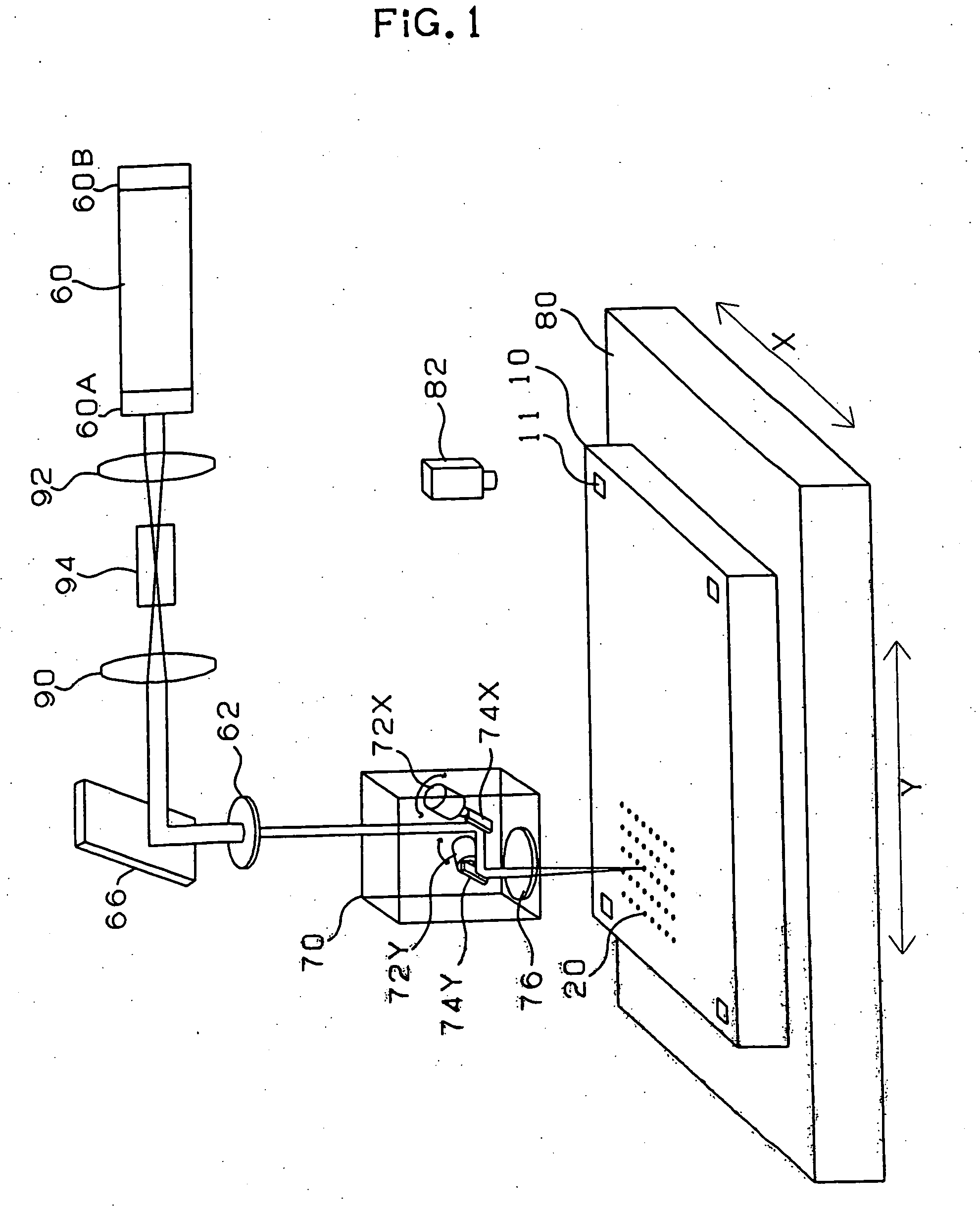
[0131]FIG. 1 shows a multilayer printed wiring board manufacturing apparatus in relation to the present invention.

[0132] In the first embodiment, as the laser source, a CO2 laser oscillator 60 which generates the CO2 laser in the wavelength of 10.6μm is used. This CO2 laser oscillator 60 is designed as the resonator type oscillator formed by sealing the CO2 gas between a total reflection mirror 60B and a partial reflection mirror 60A. An energy from the excited CO2 is emitted as the laser beam via the partial reflection mirror 60A.

[0133] The laser beam in the beam diameter of 20 mm radiated from the CO2 laser oscillator 60 is condensed by a condenser lens 92 of zinc selenium (ZnSe) coated with a thin film of sodium fluoride (manufactured by MELLES GRIOT) and is then incident to a metal tellurium 94. The surface of the condenser lens 92 is perfectly transmitting the light beam in the wavelength of 10.6 μm (AR: ANTIREFLECTION).

[0134] Tellurium 94 has the length of 5 mm and is cut in...

second embodiment

[0178] In the second embodiment, the CO2 laser oscillator 260 in the wavelength of 10.6 μm is used as the laser source. The light beam emitted from the laser oscillator 260 is sent to the galvano-head via the transfer mask 262 in order to make clear the focal point on the substrate.

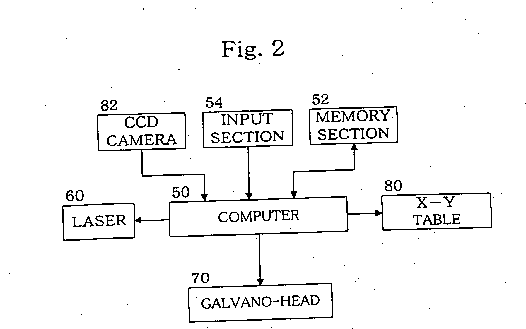
[0179] The scanning head 270 is formed of a galvano-mirror formed of a set of the galvano-mirror 274X for scanning the laser beam in the X direction and the galvano-mirror 274Y for scanning the beam in the Y direction. These mirrors 274X, 274Y are driven by the control motors 272X, 272Y. The motors 272X, 272Y adjust the angles of the mirrors 274X, 274Y according to the control command from the computer to be explained later and also transmit the detecting signal from the built-in encoder to the computer side.

[0180] The scanning area of the galvano-mirror is 30×30 mm. Moreover, the positioning speed of galvano-mirror is 400 points / sec in the scanning area. The laser beam is scanned in the X-Y directions v...

third embodiment

[0205] the present invention will be explained with reference to FIG. 12 to FIG. 17.

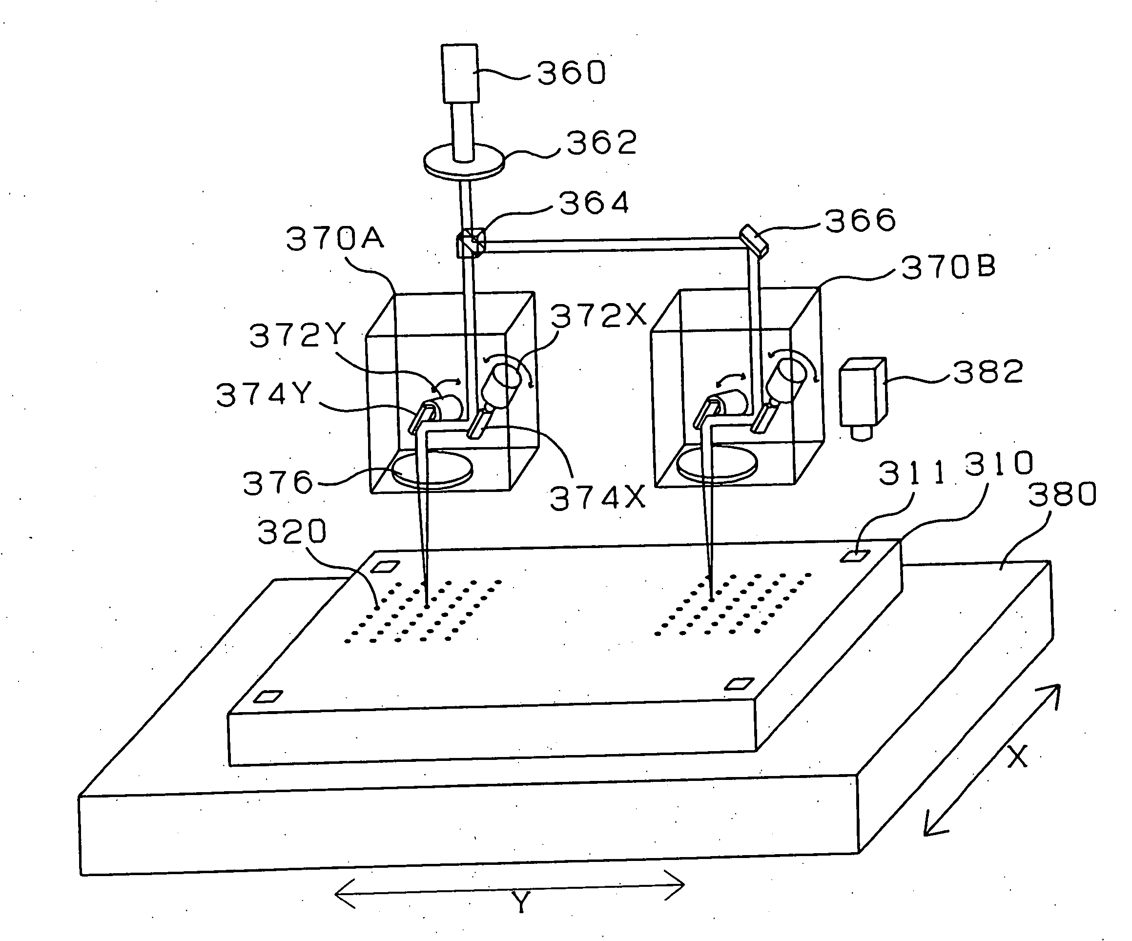
[0206]FIG. 12 shows a multilayer printed wiring board manufacturing apparatus in relation to the third embodiment of the present invention.

[0207] In this embodiment, the CO2 laser oscillator 360 is used as the laser source. The light beam emitted from the laser oscillator 360 is incident to a beam splitter 364 via the transfer mask 362 in order to make clear the focal point on the substrate. In the beam splitter 364, the incident light is distributed by 1:1 in the power ratio and is then transmitted to the side A galvano-head (scanning head) 370A and to the side B galvano-head (scanning head) 370B through reflection by the mirror 366. As the beam splitter, those combining a plurality sets of the prisms and those obtained by arranging a multilayer film on zinc-selenium (ZnSe) may be used.

[0208] The side A galvano-head 370A and side B galvano-head 370B are respectively formed of a set of galvano-mirr...


PUM

PropertyMeasurementUnit
diameteraaaaaaaaaa
diameteraaaaaaaaaa
diameteraaaaaaaaaa

Abstract

There is provided a laser processing apparatus, a multilayer printed wiring board manufacturing apparatus, and a manufacturing method to form via holes of ultra-fine diameter. The laser beam from the CO2 laser oscillator (60) is converted to the shortened wavelength beam by a tellurium crystal (94) to control diffraction of the laser beam. Simultaneously, when the laser beam is condensed, a limit value of the condensation limit is reduced. Thereby, the spot diameter of laser beam is reduced and a hole for via hole is bored on the interlayer insulation resin on a substrate (10). Therefore, even when the laser beam output is raised to form a deeper hole, the hole diameter is not widened and thereby a hole for a small diameter via hole can be formed.

Description

BACKGROUND OF THE INVENTION [0001] 1. Field of the Invention [0002] The present invention relates to a multilayer printed wiring board manufacturing apparatus and method and a laser processing apparatus, particularly to a multilayer printed wiring board manufacturing apparatus and method to form fine holes at a low cost and a laser processing apparatus. [0003] 2. Description of Related Art [0004] A build-up multilayer wiring board alternately has interlayer resin insulators and conductive circuit layers, provides holes to the interlayer resin insulator layers and then electrically connects the upper layers and lower layers by forming conductive films at the wall surface of these holes. [0005] A hole (via hole) of the interlayer resin insulating layer is generally formed through the exposure and developing process by giving photosensitive property to the interlayer resin. [0006] However, the diameter of these via holes on the multilayer printed wiring board is almost 100 μm or less a...

Claims


Application Information

Patent Timeline
Patent Type & Authority Applications(United States)
IPC IPC(8): B23K26/38B23K26/03B23K26/04B23K26/06B23K26/067B23K26/08H05K1/02H05K3/00H05K3/46
CPCB23K26/03B23K26/032B23K26/04B23K26/063B23K26/0639B23K26/0643B23K26/0648B23K26/0656B23K26/0665B23K26/067B23K26/0673B23K26/08B23K26/0807B23K26/0853B23K26/381B23K26/386B23K26/4075B23K2201/42H05K1/0269H05K3/0008H05K3/0026H05K3/0035H05K3/4644H05K3/4679H05K2201/09781H05K2201/09918H05K2201/10113B23K26/4065B23K26/4085B23K26/40B23K26/0622B23K26/064B23K26/066B23K26/082B23K26/382B23K26/389B23K2101/42B23K2103/16B23K2103/42B23K2103/50
Inventor HIRAMATSU, YASUJI
Owner IBIDEN CO LTD
Why Eureka
Try Eureka