
Optics for generation of high current density patterned charged particle beams

a charge particle and high current density technology, applied in the field of optics for generating high current density patterned electron beams, can solve the problems of long current tails, large amount of beam writing dose, and inability to meet the needs of treatment, so as to maximize process latitude and minimize the effect of beam writing dos

Active Publication Date: 2006-07-06
MULTIBEAM CORP +1
View PDF22 Cites 25 Cited by
  • Summary
  • Abstract
  • Description
  • Claims
  • Application Information

AI Technical Summary

Benefits of technology

[0020] The shaped beam generated by this column is characterized by improved current profile edge sharpness relative to a Gaussian beam, as well as a nearly square current distribution at the resist exposure dose (the latter being very desirable for lithography applications). Advantages of this apparatus include the ability to generate a shaped beam without the added complexity of shaping apertures, deflectors and lenses typically found, in variable-shaped beam columns. In addition, current densities approaching those of Gaussian beam systems are achieved, greatly reducing resist exposure times and enhancing writing throughputs in lithography applications.
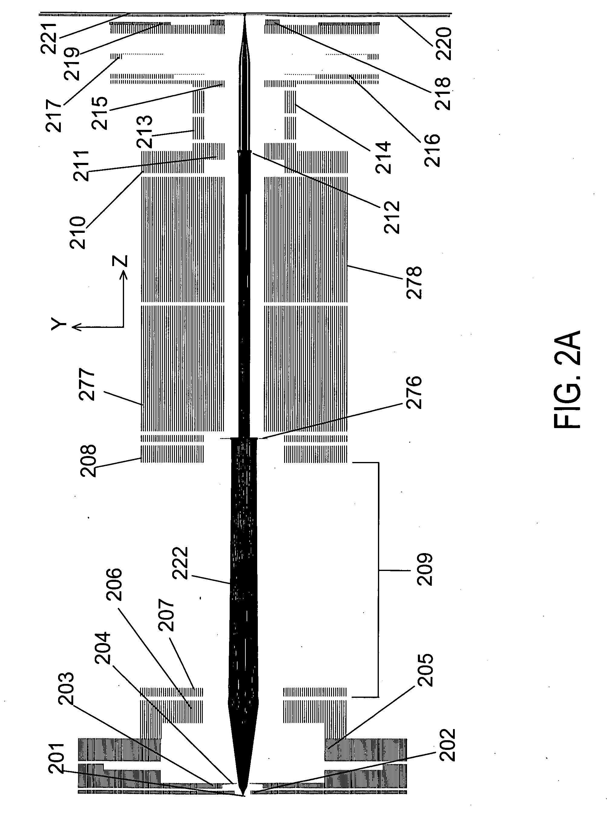
[0022] Blanking System—the apparatus disclosed herein employs a unique blanking system which does not require the use of an intermediate crossover between the electron source and the wafer. A double-deflection blanker is used to project the effective blanking plane back to the position of the virtual source. This is advantageous since the absence of an intermediate crossover substantially reduces space charge beam spreading arising from electron-electron interactions. A further advantage of the double-deflection blanker geometry is the ability to blank beams over a much wider range of beam sizes—in prior art designs, since the (single) blanker had to be positioned at the cross-over for conjugate blanking, it was not possible to achieve the wide range of beam sizes (<30 nm to >120 nm) possible with the present invention since such a wide size range necessitates moving the cross-over to various (widely-spaced) positions along the optical axis in order to vary the column magnification. Another novel aspect of the blanking system is the use of a square beam-trimming aperture above the blankers to reduce the beam size and shape the beam into a square cross-section. This has the advantage that the beam is shaped to be only slightly larger than the PBDA (which also serves as the blanking aperture) thereby maximizing the attainable blanking speed. In addition, a square beam, when swept across the PBDA, will uniformly illuminate every part of the PBDA openings, thereby making the deposited current on the wafer more uniform within the shaped beam.
[0023] Main Deflectors—the present invention employs a unique main deflector design, optimized for the requirement to deflect the patterned beam a much larger distance off-axis in one direction (typically >25 μm) than in the other direction (˜1 μm). The deflector design employs a large number of separate electrodes (22 in the embodiment herein), but requires only four drive signals. The arrangement of the 22 deflector electrodes simulates the electric field generated by a set of parallel plates, which is more uniform than is possible with prior art octupole designs. A more uniform electric field reduces the deflection aberrations induced in the beam, enabling sharper edge profiles in the patterned beam of the invention described herein. Prior art deflectors employ symmetrical octupole designs which would have increased aberrations for the large deflections required here.
[0024] Main Lens Design—to form a shaped high current-density beam on the wafer surface across a wide range of positions off-axis (at least 25 μm), the present invention employs a main lens structure in which the effective axis of the lens can be moved in synchrony with the deflection of the beam so that the beam always appears to be on the optical axis of the main lens. The lens structure of the present invention employs two sets of octupole electrodes integrated within the lens structure to add small transverse dipole fields to the generally axial electric fields of the lens. These dipole fields can offset the axial field by >25 μm in order to center the lens on the beam. Thus, the beam always undergoes a focusing effect nearly identical to that found on axis. This is advantageous since all off-axis aberrations, both geometrical (coma, astigmatism, curvature of field, distortion) and chromatic (variation in magnification) are essentially eliminated, thereby improving the edge sharpness of the patterned beam. Prior art systems employing “moving lenses” required much more complicated electrode designs than those employed herein.

Problems solved by technology

This method has the advantage that the scan electronics is typically simpler, but the disadvantage is that the beam may spend large amounts of time moving across areas not needing to be exposed.
This method has the advantage of reduced time over areas not needing to be exposed, but the disadvantage of more complicated and expensive deflection electronics.
A key disadvantage of Gaussian beams is their long tails of current, stretching far outside the central beam diameter—only 50% of the beam current at the substrate falls within the FWHM of a two-dimensional Gaussian distribution.
Either of the two approaches to beam positioning can be combined with either of the two approaches to beam shaping, but none of these four combinations is capable of fully meeting the semiconductor industry's needs.

Method used


Image

  • Optics for generation of high current density patterned charged particle beams
  • Optics for generation of high current density patterned charged particle beams
  • Optics for generation of high current density patterned charged particle beams

Examples


Embodiment Construction

[0093] This invention will be discussed in detail using its implementation in the field of electron beam lithography as an illustrative example. However, many other fields of use are envisaged, as outlined immediately below.

[0094] Scanning electron microscopy typically utilizes a roughly Gaussian beam in order to maximize the beam current density, thereby minimizing imaging time and / or maximizing the image signal-to-noise ratio. The disadvantage of using a Gaussian beam for microscopy is the long current tails extending away from the center of the beam which tend to reduce the achievable image contrast. The present invention has potential uses in scanning electron microscopy to reduce the extent of these current tails, thus improving image contrast. These same considerations would apply to many types of scanned electron beam imaging and analysis tools, such as Scanning Auger Microscopes, Scanning Electron Microscopes, Scanning Transmission Electron Microscopes, etc.

[0095] The pres...


PUM


Abstract

A direct-write electron beam lithography system employing a patterned beam-defining aperture to enable the generation of high current-density shaped beams without the need for multiple beam-shaping apertures, lenses and deflectors is disclosed. Beam blanking is accomplished without the need for an intermediate crossover between the electron source and the wafer being patterned by means of a double-deflection blanker, which also facilitates proximity effect correction. A simple type of “moving lens” is utilized to eliminate off-axis aberrations in the shaped beam. A method for designing the patterned beam-defining aperture is also disclosed.

Description

CROSS-REFERENCE TO RELATED APPLICATIONS [0001] This application claims the benefit of U.S. Provisional Application Ser. No. 60 / 509,582 filed Oct. 7, 2003 and U.S. Provisional Application Ser. No. 60 / 582,014 filed Jun. 21, 2004, both incorporated by reference herein.BACKGROUND OF THE INVENTION [0002] 1. Field of the Invention [0003] This invention relates to the field of charged particle optics, and in particular to methods and systems for generation of high current density shaped electron beams. [0004] 2. Description of the Related Art [0005] The use of electron beams to lithographically pattern semiconductor masks, reticles and wafers is an established technique. The different writing strategies used may be characterized by a few key parameters: BEAM POSITIONING STRATEGY [0006] There are two main approaches to the positioning of electron beams for the exposure of resist during the lithographic process: [0007] (a) Raster Scanning, where the beam is moved on a regular two-dimensional...

Claims


Application Information

Patent Timeline
IPC IPC(8): G21K5/10
CPCB82Y10/00B82Y40/00H01J37/3174H01J2237/043H01J2237/1534
Inventor PARKER, N. WILLIAM
Owner MULTIBEAM CORP
Learn More