Strained channel CMOS device with fully silicided gate electrode

a gate electrode and strained channel technology, applied in the direction of basic electric elements, semiconductor devices, electrical equipment, etc., can solve the problems of increasing the critical dimension of the device, affecting the drive current of the gate sheet, and increasing the delay time of signal propagation

Inactive Publication Date: 2006-07-06
TAIWAN SEMICON MFG CO LTD
View PDF3 Cites 63 Cited by
  • Summary
  • Abstract
  • Description
  • Claims
  • Application Information

AI Technical Summary

Problems solved by technology

In addition, drive current is affected by gate sheet resistance.
Thus the higher the sheet resistance of the gate electrode, the larger the delay time in signal propagation.
In addition, due to complex relationships between the thickness of a silicide, which remains about constant with device scaling, and scaling size reductions of the CMOS device, for example including a junction depth of source and drain regions, the problem of current leakage (diode leakage) becomes increasingly problematical at smaller device critical dimensions.
Thus, prior art...

Method used


Image

  • Strained channel CMOS device with fully silicided gate electrode
  • Strained channel CMOS device with fully silicided gate electrode
  • Strained channel CMOS device with fully silicided gate electrode

Examples


Embodiment Construction

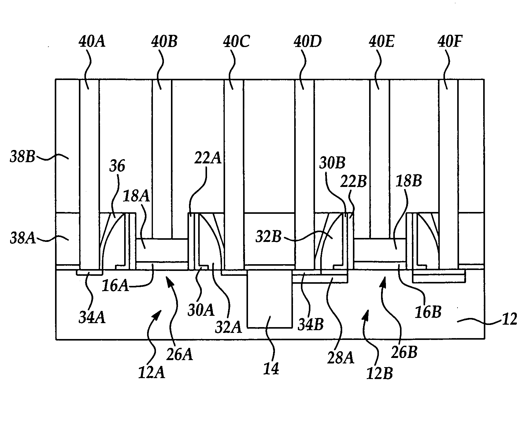
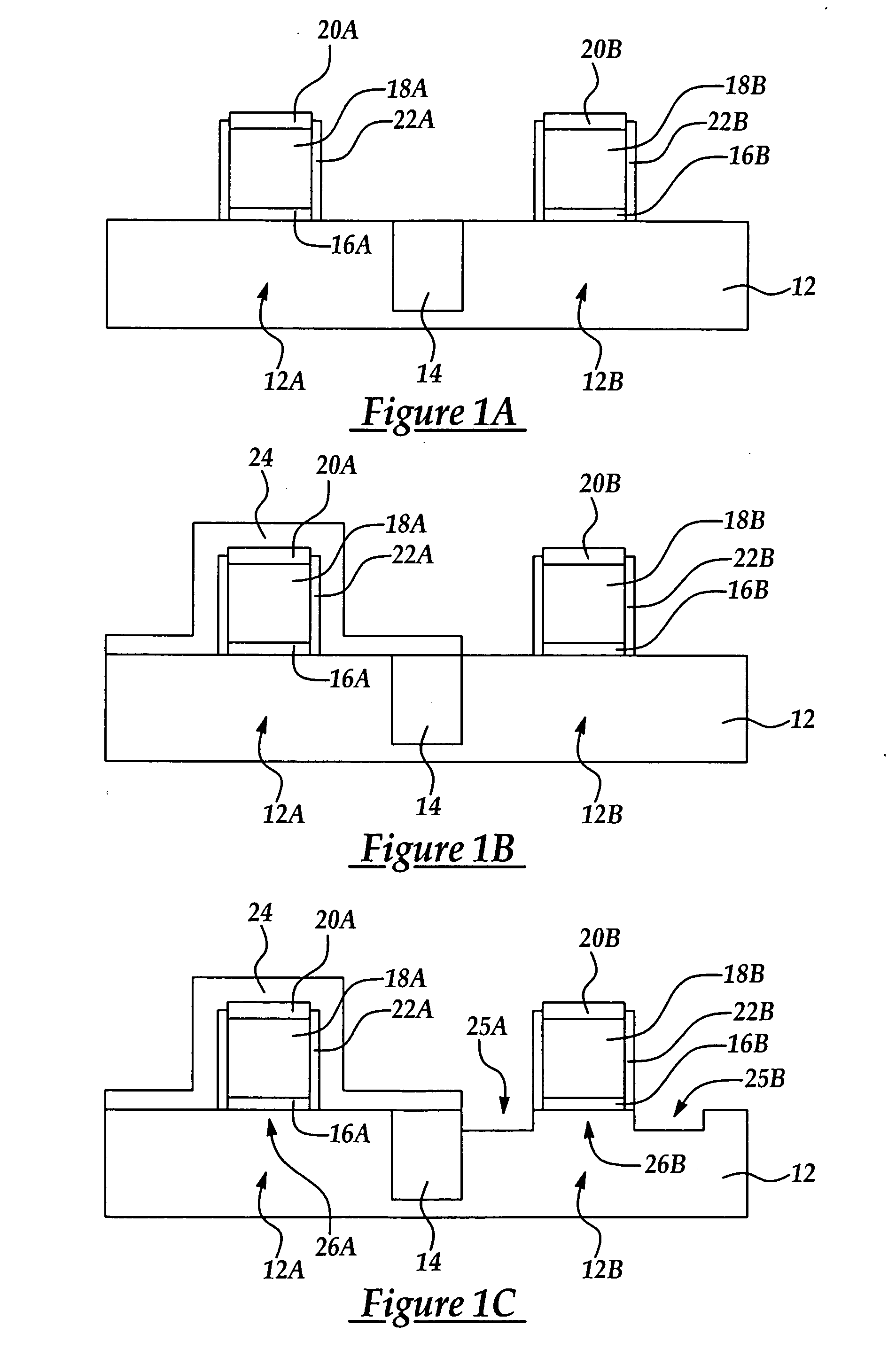
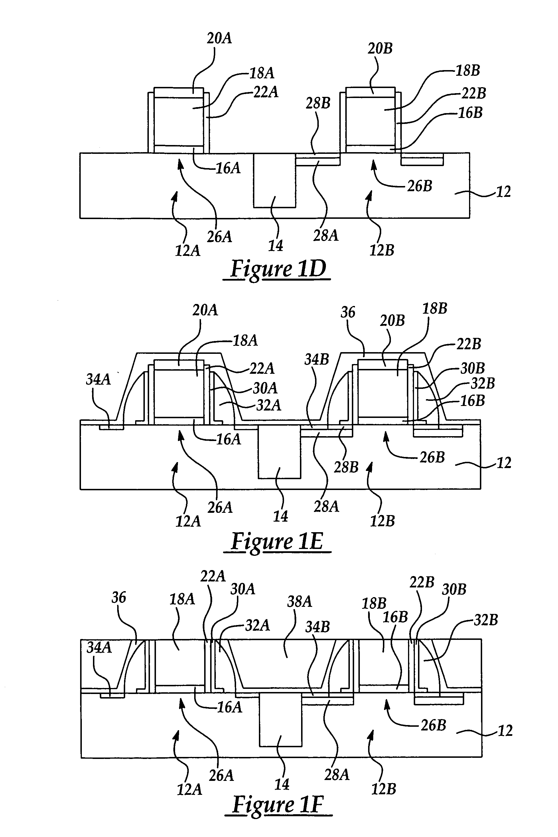
[0014] Although the method of the present invention is explained with reference to exemplary NMOS and PMOS MOSFET devices, it will be appreciated that aspects of the present invention may be applied to the formation of any MOSFET device including dual gate or twin gate CMOS inverters where a fully silicided gate electrode is formed to reduce a gate electrode resistance and avoid a poly-depletion effect. It will be appreciated that additional benefits are realized by forming a strained channel region to improve charge carrier mobility, both processes advantageously improving device performance including drive current (Idsat) and device speed.

[0015] Referring to FIGS. 1A-1H in an exemplary process flow for forming the fully silicided gate electrode CMOS structures of the present invention, are shown cross-sectional schematic views of a portion of a semiconductor wafer at stages of an exemplary production process.

[0016] For example, referring to FIG. 1A, is shown a semiconductor subs...


PUM


Abstract

A strained channel NMOS and PMOS device pair including fully silicided gate electrodes and method for forming the same, the method including providing a semiconductor substrate including NMOS and PMOS device regions including respective gate structures including polysilicon gate electrodes; forming recessed regions on either side of a channel region including at least one of the NMOS and PMOS device regions; backfilling portions of the recessed regions with a semiconducting silicon alloy to exert a strain on the channel region; forming offset spacers on either side of the gate structures; thinning the polysilicon gate electrodes to a silicidation thickness to allow full metal silicidation through the silicidation thickness; ion implanting the polysilicon gate electrodes to adjust a work function; and, forming a metal silicide through the silicidation thickness to form metal silicide gate electrodes.

Description

FIELD OF THE INVENTION [0001] This invention generally relates to formation of MOSFET devices in integrated circuit manufacturing processes and more particularly to a strained channel NMOS and PMOS device pair and method of forming the same including fully silicided gate electrodes to improve a drive current. BACKGROUND OF THE INVENTION [0002] As is well known, increased device density, together with higher speed performance and lower power consumption are major driving forces in integrated circuit manufacturing. CMOS design consideration for high speed digital applications are usually determined by the pull up time and pull down time of each individual gate. Individual gates are associated with a delay time period for signal propagation in PMOS and NMOS gate electrodes. The delay time period, in turn, is inversely proportional to the drive current (Idrive). It is therefore clear that maximizing the drive current will increase the performance speed or Figure of Merit (FOM) of a CMOS...

Claims


Application Information

Patent Timeline
IPC IPC(8): H01L21/8238
CPCH01L21/823807H01L21/823814H01L21/823828H01L29/66545H01L29/66636H01L29/7842H01L29/7843H01L29/7848Y10S438/938
Inventor CHAN, BOR-WENCHIU, YUAN-HUNGTAO, HAN-JAN
Owner TAIWAN SEMICON MFG CO LTD
Why Eureka
Try Eureka