Semiconductor apparatus and fabrication method of the same

a technology of semiconductors and fabrication methods, applied in semiconductor/solid-state device details, identification means, instruments, etc., can solve the problems of easy cracking and heavy, glass substrates, quartz substrates, etc., and achieve the effect of preventing deterioration

Active Publication Date: 2006-08-24
SEMICON ENERGY LAB CO LTD
View PDF26 Cites 16 Cited by
  • Summary
  • Abstract
  • Description
  • Claims
  • Application Information

AI Technical Summary

Benefits of technology

[0012] In view of the foregoing, it is an object of the present invention to provide a semiconductor apparatus capable of preventing deterioration due to penetration of moisture or oxygen, for example, a light-emitting apparatus having an organic light-emitting device that is formed over a plastic substrate, and a liquid crystal display apparatus using a plastic substrate.
[0013] According to the present invention, devices formed on a glass substrate or a quartz substrate (a TFT, a light-emitting device containing an organic compound, a liquid crystal device, a memory device, a thin-film diode, a pin-junction silicon photoelectric converter, a silicon resistance element, or the like) are separated from the substrate, and transferred to a plastic substrate having high thermal conductivity. The present invention provides a device of long lifetime by radiating heat generated in the device through the plastic substrate having high thermal conductivity.

Problems solved by technology

Although a glass substrate, a quartz substrate, or the like is used in many image display apparatuses at present, it has disadvantages that they are easy to crack and heavy.
Further, the glass substrate, the quartz substrate, or the like is unsuitable for mass production since it is difficult to be enlarged.
However, since the heat resistance of the plastic film is low, the highest temperature during process is required to be low, consequently, it is impossible at present to form the TFT that has high electric characteristics compared with the one being formed over a glass substrate.
Hence, no high-performance liquid crystal display apparatus and light-emitting device using a plastic film has been realized.
An organic light-emitting layer is deteriorated due to these impurities, so that lifetime of a light-emitting apparatus becomes reduced.
In addition, a substrate such as plastic films or the like is weak against heat generally.
Further, too low deposition temperature causes decline in quality of the film and difficulty of preventing penetration of moisture or oxygen into a light-emitting device.
There is also a problem of deforming and deterioration of a part of a substrate due to localized heat generation during driving of the device that is formed over a substrate such as plastic films or the like.

Method used


Image

  • Semiconductor apparatus and fabrication method of the same
  • Semiconductor apparatus and fabrication method of the same
  • Semiconductor apparatus and fabrication method of the same

Examples


embodiment mode 1

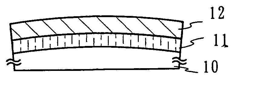
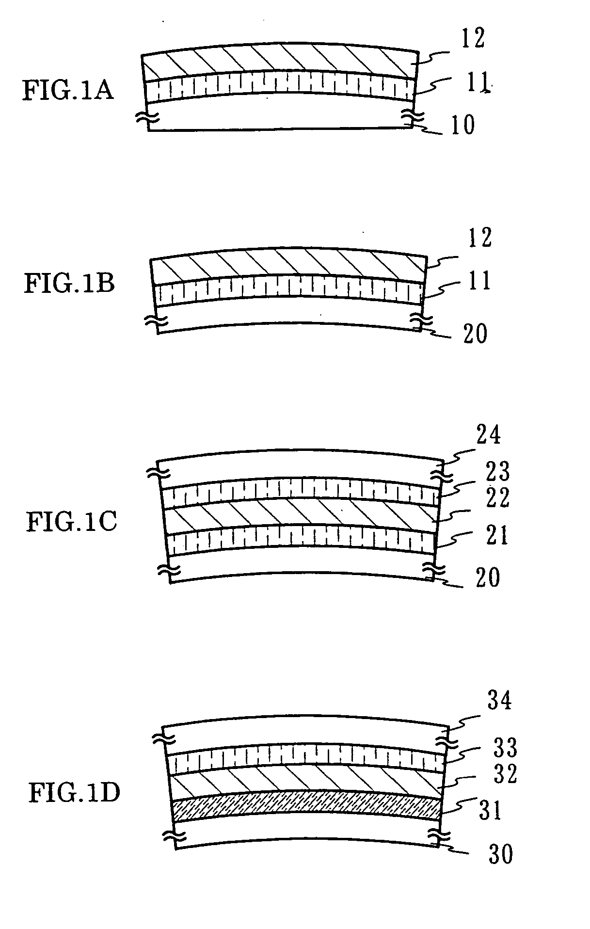
[0084] An example of bonding an insulating substrate having high thermal conductivity or a substrate to a release layer (including a device) that is separated by peeling-off method will be described in this embodiment mode.

[0085] In FIG. 1A, reference numeral 10 denotes an insulating substrate having thermal conductivity; 11, an adhesive; and 12, a release layer (including a device). The release layer 12 includes a semiconductor device formed on a substrate (not shown) in advance. The release layer 12 is separated from a substrate by a peeled-off method and bonded to the substrate 10 with the adhesive 11.

[0086] Specified quantity of powder such as Al, Mg, ceramics, or the like, and powder of a low-melting metal (lead-free solders) are mixed into polyphenylene sulfide or the like as thermoplastic resin, and the mixture is pelletized. The resulted pellets may be formed into the substrate 10 having a curved surface by injection molding process or compression molding process. The low-...

embodiment mode 2

[0094] An example of manufacturing an active matrix light emitting apparatus will be described with reference to FIG. 3 in this embodiment mode 2.

[0095] The present invention can be applied to an active matrix light-emitting apparatus, but not exclusively, any light-emitting device as long as that has a layer containing an organic compound such as a passive matrix light-emitting apparatus for a color display panel, a surface luminous, or an area color light-emitting apparatus for electric spectaculars device.

[0096] First, a device is formed on a glass substrate (a first substrate 300). A metal film 301, which is a tungsten film (having a thickness ranging from 10 to 200 nm, preferably, from 50 to 75 nm) here, is formed on the glass substrate by sputtering, and an oxide film 302, which is a silicon oxide film (having a thickness ranging from 150 to 200 nm) here, is stacked thereon without exposing to the air. The tungsten film and the silicon oxide films are formed over the edge po...

embodiment mode 3

[0122] An example of a method for manufacturing a light-emitting apparatus in which light generated in a light-emitting device is extracted through a first electrode will be described. Since partway of this embodiment mode is the same as Embodiment Mode 2, further explanation will be omitted, and like components are denoted by like numerals as of Embodiment Mode 2.

[0123] The process up to peeling-off the first substrate is the same as Embodiment Mode 2. Note that a transparent conductive film is used for a first electrode 304 in order to transmit light.

[0124] When the state shown in FIG. 4D is achieved according to Embodiment Mode 2, a transparent plastic substrate 412 is bonded thereto with an adhesive 411 (FIG. 4E).

[0125] A second substrate 308 is separated from the two-sided tape 307 (FIG. 4F).

[0126] Then, the two-sided tape 307 is removed (FIG. 4G).

[0127] And then, the film formed of water-soluble resin 306 is melted by water and removed (FIG. 4H). If residue of the water-s...


PUM

PropertyMeasurementUnit
thicknessaaaaaaaaaa
thicknessaaaaaaaaaa
thicknessaaaaaaaaaa

Abstract

It is an object of the present invention to provide a semiconductor device capable of preventing deterioration due to penetration of moisture or oxygen, for example, a light-emitting apparatus having an organic light-emitting device that is formed over a plastic substrate, and a liquid crystal display apparatus using a plastic substrate. According to the present invention, devices formed on a glass substrate or a quartz substrate (a TFT, a light-emitting device having an organic compound, a liquid crystal device, a memory device, a thin-film diode, a pin-junction silicon photoelectric converter, a silicon resistance element, or the like) are separated from the substrate, and transferred to a plastic substrate having high thermal conductivity.

Description

CROSS-REFERENCE TO RELATED APPLICATIONS [0001] This application is a divisional application of U.S. application Ser. No. 10 / 685,398, filed Oct. 16, 2003, now allowed, which claims the benefit of a foreign priority application filed in Japan as Serial No. 2002-305084 on Oct. 18, 2002. This application claims priority to each of these prior applications, and the disclosures of the prior applications are considered part of (and are incorporated by reference in) the disclosure of this application.BACKGROUND OF THE INVENTION [0002] 1. Technical Field [0003] The present invention relates to a semiconductor apparatus comprising a circuit composed of a device as typified by a thin film transistor (hereinafter, TFT) that is formed by means of bonding a release layer to a substrate to be transferred thereto and a method for manufacturing the semiconductor apparatus. The present invention relates, for example, to an electrooptical device such as a liquid crystal module, a light emitting appara...

Claims


Application Information

Patent Timeline
Patent Type & Authority Applications(United States)
IPC IPC(8): H01L29/08G02F1/1333G02F1/1368G09F9/00G09F9/30H01L21/02H01L21/336H01L21/77H01L21/84H01L27/12H01L27/32H01L29/786H01L51/00H01L51/50H01L51/52H05B33/02H05B33/04H05B33/10H05B33/14
CPCH01L27/12H01L27/1214H01L2924/0002H01L27/1266H01L27/3244H01L27/3281H01L29/78603H01L51/003H01L51/0097H01L51/524H01L51/529H01L51/56H01L2221/68368H01L2227/326H01L2251/5338Y02E10/549H01L23/12H01L2924/00H01L27/1218Y02P70/50H10K59/12H10K59/17H10K71/80H10K77/111H10K50/841H10K50/87H10K59/1201H10K2102/311H10K71/00
Inventor YAMAZAKI, SHUNPEITAKAYAMA, TORUMARUYAMA, JUNYAOHNO, YUMIKO
Owner SEMICON ENERGY LAB CO LTD
Why Eureka
Try Eureka