Method and apparatus for non-aggressive plasma-enhanced vapor deposition of dielectric films

a dielectric film, plasma-enhanced technology, applied in chemical vapor deposition coatings, electric discharge tubes, coatings, etc., can solve the problems of unsuitability for use, the method cannot be used for substrates that can withstand high temperatures without significant degradation, and the effect of reducing the flow of charged particles

Inactive Publication Date: 2006-08-24
TEGAL CORP
View PDF13 Cites 0 Cited by
  • Summary
  • Abstract
  • Description
  • Claims
  • Application Information

AI Technical Summary

Benefits of technology

[0017] In order to achieve these objects, and others, a first aspect of the invention provides a particular method of depositing dielectric films by plasma-enhanced chemical vapor deposition, in which a substrate is exposed in a vacuum to a flow of particles generate

Problems solved by technology

Traditional chemical vapor deposition methods, which are in widespread use for depositing films on substrates, lead to the substrates becoming heated to high temperatures.
Such methods can therefore be used only for substrates that withstand high temperatures without significant degradation.
Such a deposit can be applied at a lower temperature, of the order of 250° C. to 400° C. However, most plasma sources lead to performing the method at a temperature which is still too high for certain fragile semiconductor substrates, and the semiconductor components made in this way present progressive aging defects which rapidly make them unsuitable for use.
Rapid and unacceptable aging is also observed on items having

Method used


Image

  • Method and apparatus for non-aggressive plasma-enhanced vapor deposition of dielectric films
  • Method and apparatus for non-aggressive plasma-enhanced vapor deposition of dielectric films
  • Method and apparatus for non-aggressive plasma-enhanced vapor deposition of dielectric films

Examples


Embodiment Construction

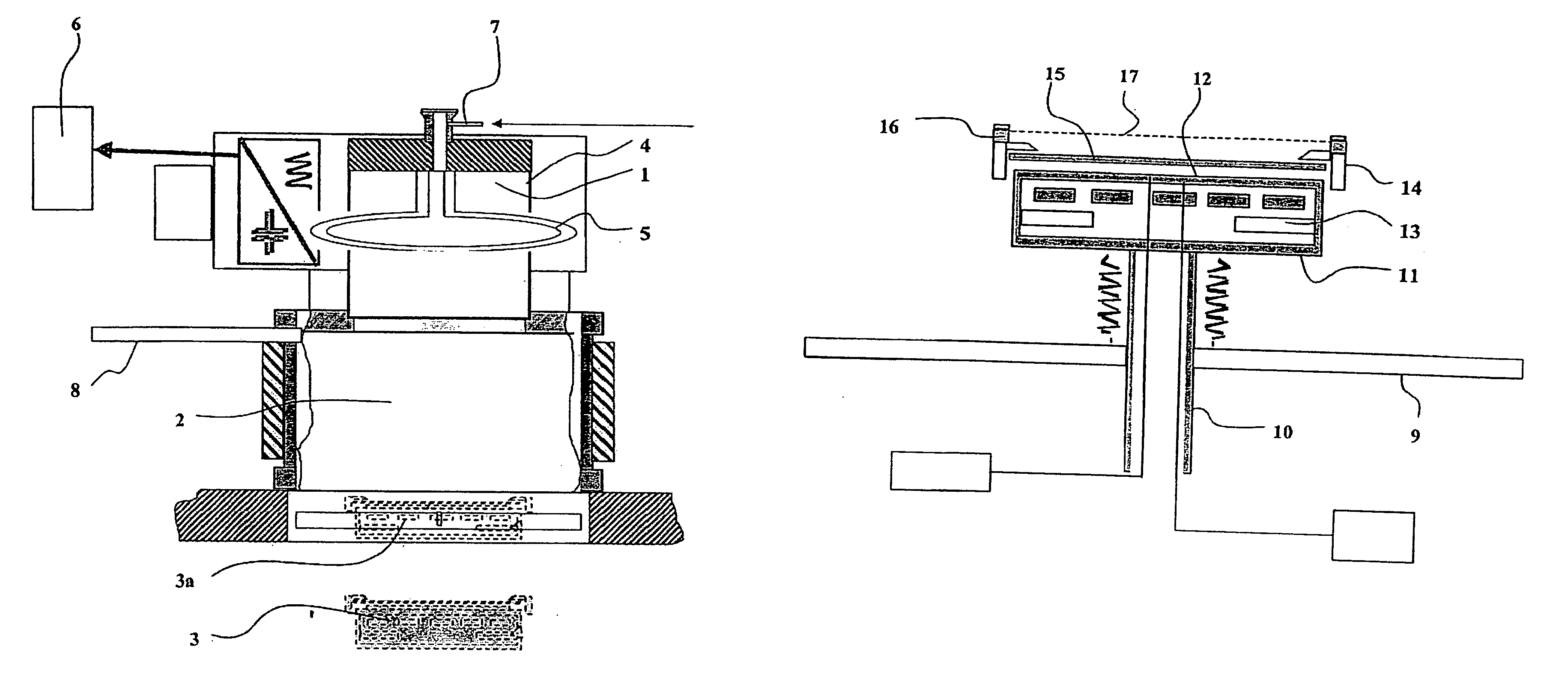
[0043] Reference is made initially to FIG. 1. Apparatus for plasma-enhanced chemical vapor deposition of a dielectric film comprises a plasma source 1, preferably a high-density ion source in order to be capable of operating properly at a lower operating temperature, followed by a diffusion chamber 2 having a substrate support 3 adapted to hold the substrate for treatment and to be engaged in the diffusion chamber 2, as shown in position 3a.

[0044] The plasma source 1 is constituted by an enclosure whose wall 4 is made of dielectric material, it is advantageously cylindrical in shape, being associated with a loop antenna 5 powered by a radiofrequency (RF) electrical generator 6. A gas inlet 7 is provided at the proximal end of the plasma source 1, i.e. at its end remote from the diffusion chamber 2.

[0045] The plasma source 1 communicates with the diffusion chamber 2 which is itself adapted to direct the plasma towards a substrate held on the substrate support in position 3a.

[0046]...


PUM

PropertyMeasurementUnit
Lengthaaaaaaaaaa
Dielectric polarization enthalpyaaaaaaaaaa
Densityaaaaaaaaaa

Abstract

While performing plasma-enhanced chemical vapor deposition on a substrate by exposing the substrate in a vacuum to a flow of particles generated by a plasma, which particles react to form a passivation layer on the substrate, a grid is interposed between the plasma and the substrate, thereby reducing the flow of charged particles towards the substrate while conserving a flow of neutral particles. The grid is formed of metal wires that are crossed at a pitch that is less than two or three times the Debye length (λD) of the plasma used, at least at the beginning of deposition. The aging properties of semiconductor components made by such a method is thereby improved.

Description

[0001] This is a divisional application of U.S. application Ser. No. 10 / 902,582, filed Jul. 30, 2004, the disclosure of which is incorporated herein.BACKGROUND OF THE INVENTION [0002] The present invention relates to methods of fabricating semiconductor components in which at least one step of plasma-enhanced chemical vapor deposition is performed consisting in exposing a semiconductor substrate in a vacuum to a flow of particles generated by a plasma, the particles reacting to form a passivation layer on the substrate of a material that has dielectric properties. [0003] Traditional chemical vapor deposition methods, which are in widespread use for depositing films on substrates, lead to the substrates becoming heated to high temperatures. Such methods can therefore be used only for substrates that withstand high temperatures without significant degradation. [0004] To make deposits on substrates that are relatively fragile, it is common practice to use plasma-enhanced chemical vapor...

Claims


Application Information

Patent Timeline
IPC IPC(8): H01L21/31H01L21/469C23C16/34C23C16/452H01L21/318
CPCC23C16/345C23C16/452H01J37/32357H01J37/32422Y10S438/932
Inventor JANY, CHRISTOPHEPUECH, MICHEL
Owner TEGAL CORP
Why Eureka
Try Eureka