Group III-V nitride-based semiconductor substrate and method of making same

a semiconductor substrate and nitride technology, applied in the direction of crystal growth process, crystal growth process, chemically reactive gas, etc., can solve the problems of non-uniform carrier concentration and electrical resistivity, non-uniform in-plane polishing speed, and non-uniform growth speed, so as to improve the uniformity of in-plane properties

Inactive Publication Date: 2006-10-12
HITACHI CABLE
View PDF18 Cites 35 Cited by
  • Summary
  • Abstract
  • Description
  • Claims
  • Application Information

AI Technical Summary

Benefits of technology

[0015] It is an object of the invention to provide a group III-V nitride-based semiconductor substrate and a method of the same that can offer an improved uniformity in in-plane property.

Problems solved by technology

First, the non-uniformity in growth temperature causes non-uniformity in growth speed.
Furthermore, if the growth speed is varied, a dopant introduction density is also varied, which causes non-uniformity in carrier concentration and electrical resistivity.
In addition, although a GaN crystal after growth is generally polished at both faces thereof to be used for a wafer, the in-plane polishing speed may be non-uniform due to a difference in dislocation density or carrier concentration and, thereby, the final thickness may be non-uniform.
Second, the non-uniformity in growth temperature causes a warp in crystal.

Method used


Image

  • Group III-V nitride-based semiconductor substrate and method of making same
  • Group III-V nitride-based semiconductor substrate and method of making same
  • Group III-V nitride-based semiconductor substrate and method of making same

Examples


##ventive example 1

INVENTIVE EXAMPLE 1

Preventing the Warping by a Thick Sapphire

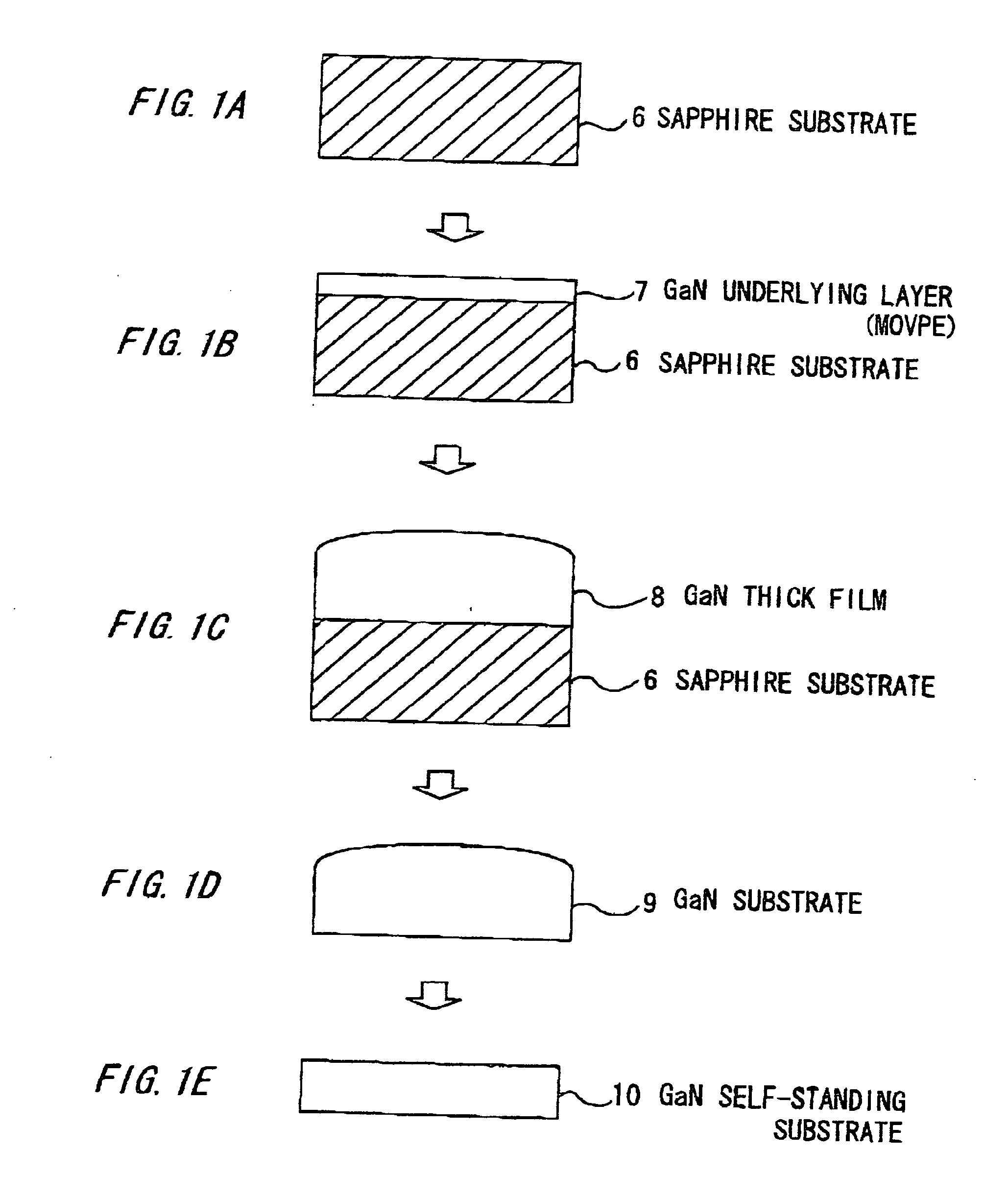
[0087]FIGS. 1A to 1E are illustrative cross sectional views showing of a method of making a group III-V nitride semiconductor substrate in the first preferred embodiment according to the invention.

[0088] As shown in FIGS. 1A and 1B, a 300 nm thick GaN underlying layer 7 is formed on a c-face sapphire substrate 6 with a diameter of 7.62 cm (=3 inches) and a thickness of 650 μm by MOVPE.

[0089] Then, like the conventional example, it is placed in a HVPE furnace and a Si-doped GaN thick film 8 is grown (FIG. 1C). Carrier gas is N2:H2=1:1. Partial pressures are GaCl=9×10⁻³ atm, NH3=1×10⁻¹ atm. For n-type doping, SiH2Cl2 gas is flown at partial pressure of 5×10⁻⁴ atm. Growth temperature is 1070° C.

[0090] By irradiating YAG laser from the backside of the sapphire substrate 6, a GaN substrate 9 is separated decomposing a GaN crystal at the interface (FIG. 1D).

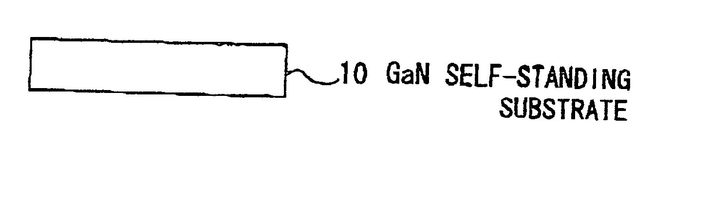
[0091] The resultant GaN crystal (i.e., GaN thick film 8) has a thi...

##ventive example 2

INVENTIVE EXAMPLE 2

Further Enhancing the Uniformity by Coating Carbon on the Back Face of the Sapphire Substrate

[0094] In the inventive example 1, an about 1 μm thick carbon layer is formed on the back face of the sapphire substrate 6 and then the HVPE growth is conducted in like manner. Thereby, the temperature distribution during growth can be further improved The thickness distribution as grown is 800 μm at the central portion and 750 μm at the outermost portion,

[0095] The properties of the GaN substrate are also improved. The dislocation density is 1×107 cm−2 both at the central portion and at the outermost portion The carrier concentration is 1×1018 cm−3 both at the central portion and at the outermost portion. Further, the c-axis is inclined about ±0.18.

##ventive example 3

INVENTIVE EXAMPLE 3

Bonding the Sapphire Substrate to the Susceptor+VAS Method

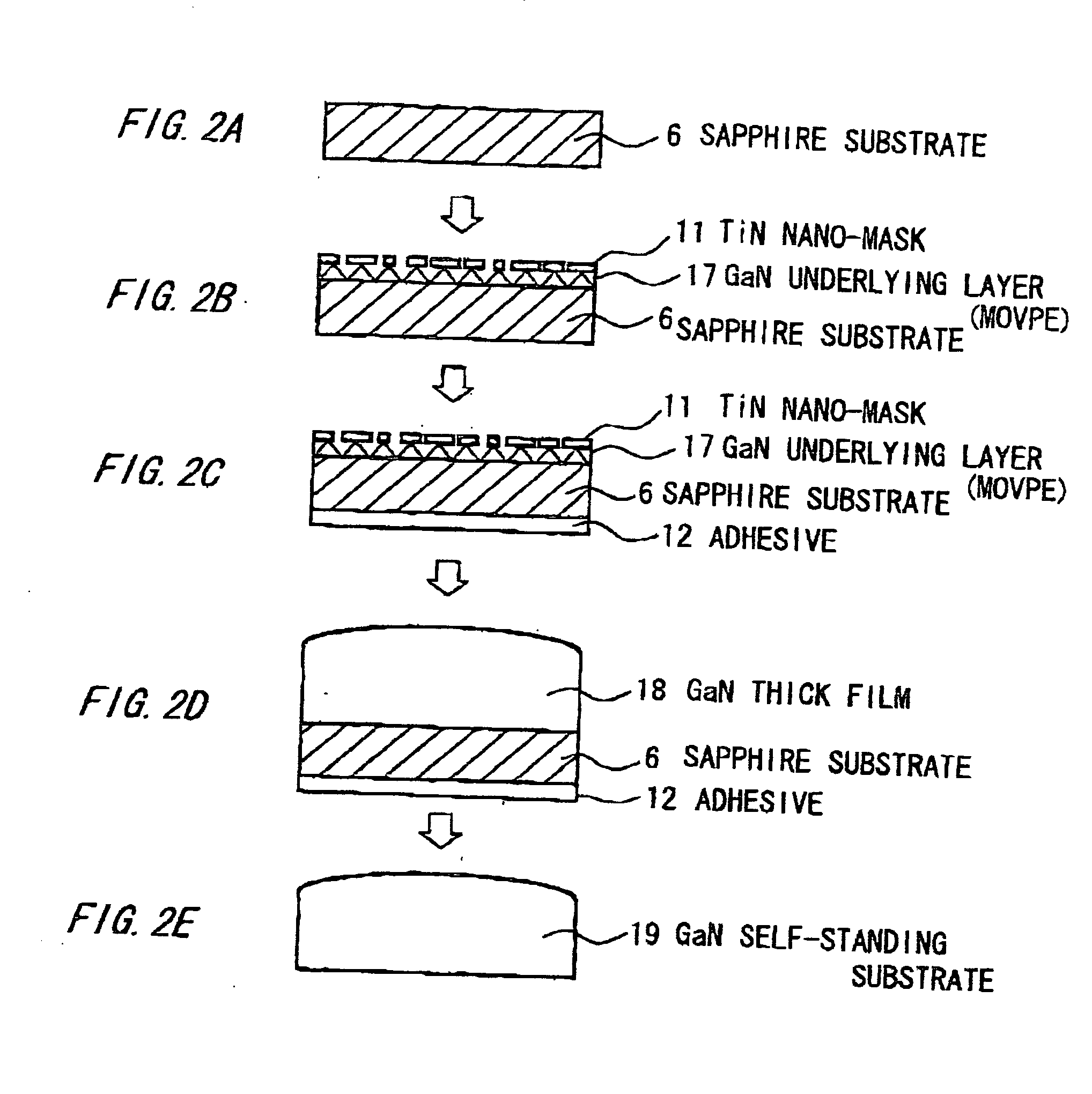
[0096]FIGS. 2A to 2E are illustrative cross sectional views showing of a method of making a group III-V nitride semiconductor substrate in the third preferred embodiment according to the invention.

[0097] As shown in FIG. 2A, a c-face sapphire substrate 6 with a diameter of 7.62 cm (=3 inches) and a thickness of 330 μm is provided.

[0098] Then, a 300 nm thick GaN thin film (=GaN under lying layer 17) is formed on the sapphire substrate 6. Then, a 20 nm thick Ti layer is formed thereon in vacuum deposition. Then, it is thermally treated in carrier gas of H2:NH3=4:1 at 1060° C. for 30 min. Thereby, the Ti layer is nitrided into a TiN layer and formed into mesh-like structure (i.e., TiN nano-mask 11) with a number of fine holes of tens of nanometers. On the other hand, the GaN underlying layer 17 is etched to have therein voids reaching up to the sapphire substrate 6 (FIG. 2B).

[0099] Then, the void-formed su...


PUM

PropertyMeasurementUnit
surface areaaaaaaaaaaa
thicknessaaaaaaaaaa
thicknessaaaaaaaaaa

Abstract

A method of making a group III-V nitride-based semiconductor substrate has the steps of: providing a first crystal substrate; placing the first crystal substrate on a susceptor; holding down the first crystal substrate on the susceptor; and growing a first group III-V nitride-based semiconductor crystal on the first crystal substrate.

Description

[0001] The present application is based on Japanese patent application No. 2005-113416, the entire contents of which are incorporated herein by reference. BACKGROUND OF THE INVENTION [0002] 1. Field of the Invention [0003] This invention relates to a group III-V nitride-based semiconductor substrate and a method of making the same. [0004] 2. Description of the Related Art [0005] GaN-based compound semiconductors such as gallium nitride (GaN), indium gallium nitride (InGaN) and aluminum gallium nitride (AlGaN) attract attention for a material of blue light emitting diode (LED) or laser diode (LD). Further, since the GaN-based compound semiconductors have a good heat resistance and environment resistance, they have begun to be applied to other electronic devices. [0006] At present, a substrate used widely to grow GaN is sapphire. In general, a method is used in which GaN is epitaxially grown on a sapphire single crystal substrate by MOVPE (metalorganic vapor phase epitaxy) etc. [0007]...

Claims


Application Information

Patent Timeline
Patent Type & Authority Applications(United States)
IPC IPC(8): H01L29/06H01L29/12
CPCC30B25/02C30B29/403H01L21/0242H01L21/02458H01L33/0075H01L21/0262H01L21/02642H01L21/02664H01L29/2003H01L21/0254
Inventor OSHIMA, YUICHI
Owner HITACHI CABLE
Why Eureka
Try Eureka