Nitride semiconductor laser element

a laser element and semiconductor technology, applied in semiconductor lasers, laser cooling arrangements, laser details, etc., can solve problems such as light leakage from waveguide regions to other regions, and achieve the effects of preventing improper operation of detectors, preventing ffp deterioration, and more stable laser ligh

Active Publication Date: 2006-11-16
NICHIA CORP
View PDF10 Cites 28 Cited by
  • Summary
  • Abstract
  • Description
  • Claims
  • Application Information

AI Technical Summary

Benefits of technology

[0037] A nitride laser semiconductor laser device according to the present invention absorbs stray light inside the substrate, and thus suppresses FFP deterioration due to mixture of the stray light into laser light. In addition, the laser device absorbs the stray light and emits luminescent radiation, and has a high reflective end surface protective film formed therein such that the luminescent radiation is not emitted outward. Therefore, the laser device can provide more stable laser light. Furthermore, a high reflective end surface protective film is also formed on the rear side to prevent improper operation of a detector due to the luminescent radiation with a wavelength longer than light emitted from the active layer, thus, precise driving control can be obtained. Therefore, it is possible to provide an excellent reliable semiconductor laser device.

Problems solved by technology

However, light leaks from the waveguide region to other regions.

Method used


Image

  • Nitride semiconductor laser element
  • Nitride semiconductor laser element
  • Nitride semiconductor laser element

Examples


example 1

[0094] The following description will describe examples. However, a device structure of the n-type nitride semiconductor layer, active layer and p-type nitride semiconductor layer that compose the nitride semiconductor layer according to the present invention is not specifically limited to them, various lamination structure can be used. Laser device structures described in the following examples can be used, however, other device structures can be applied. A III-V nitride semiconductor group semiconductor including a nitride semiconductor such as GaN, AlN and InN, and a mixture crystal of them can be employed. Additionally, A III-V nitride semiconductor group semiconductor containing B, P, and so on, can be used. Any known methods that grows a nitride semiconductor, such as MOVPE, MOCVD (metalorganic chemical vapor deposition), HVPE (halide vapor-phase epitaxiay), MBE (molecular beam epitaxy), and so on, can be used for growth of the nitride semiconductor.

(Nitride Semiconductor Su...

example 2

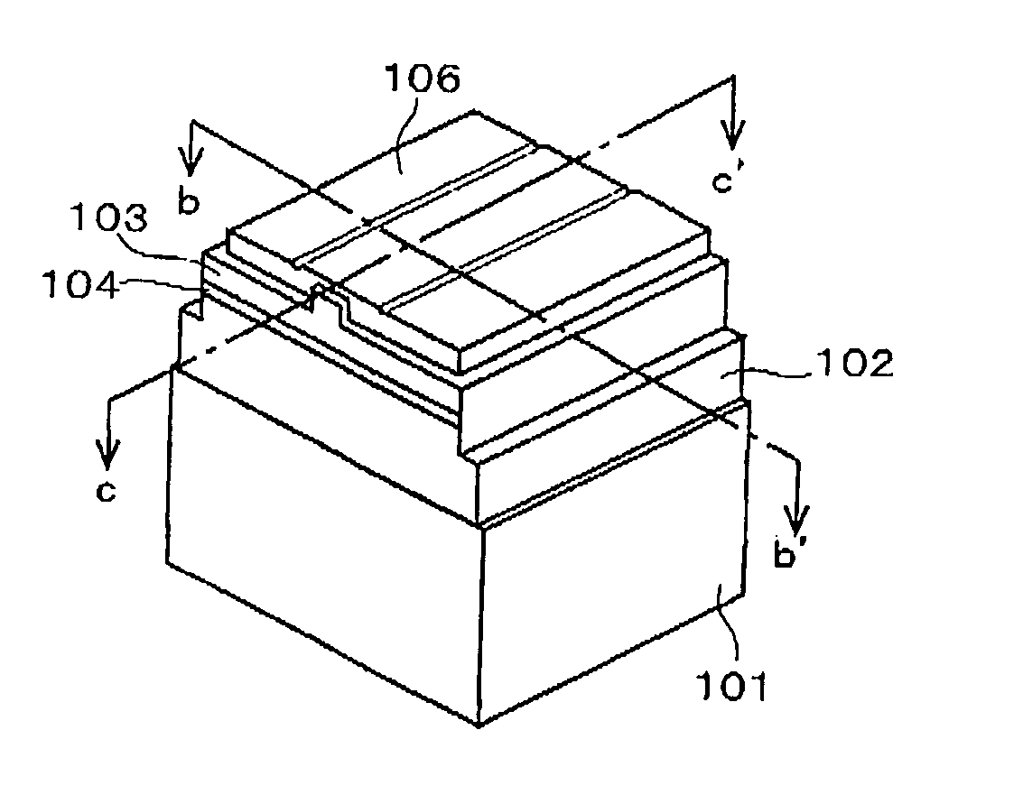
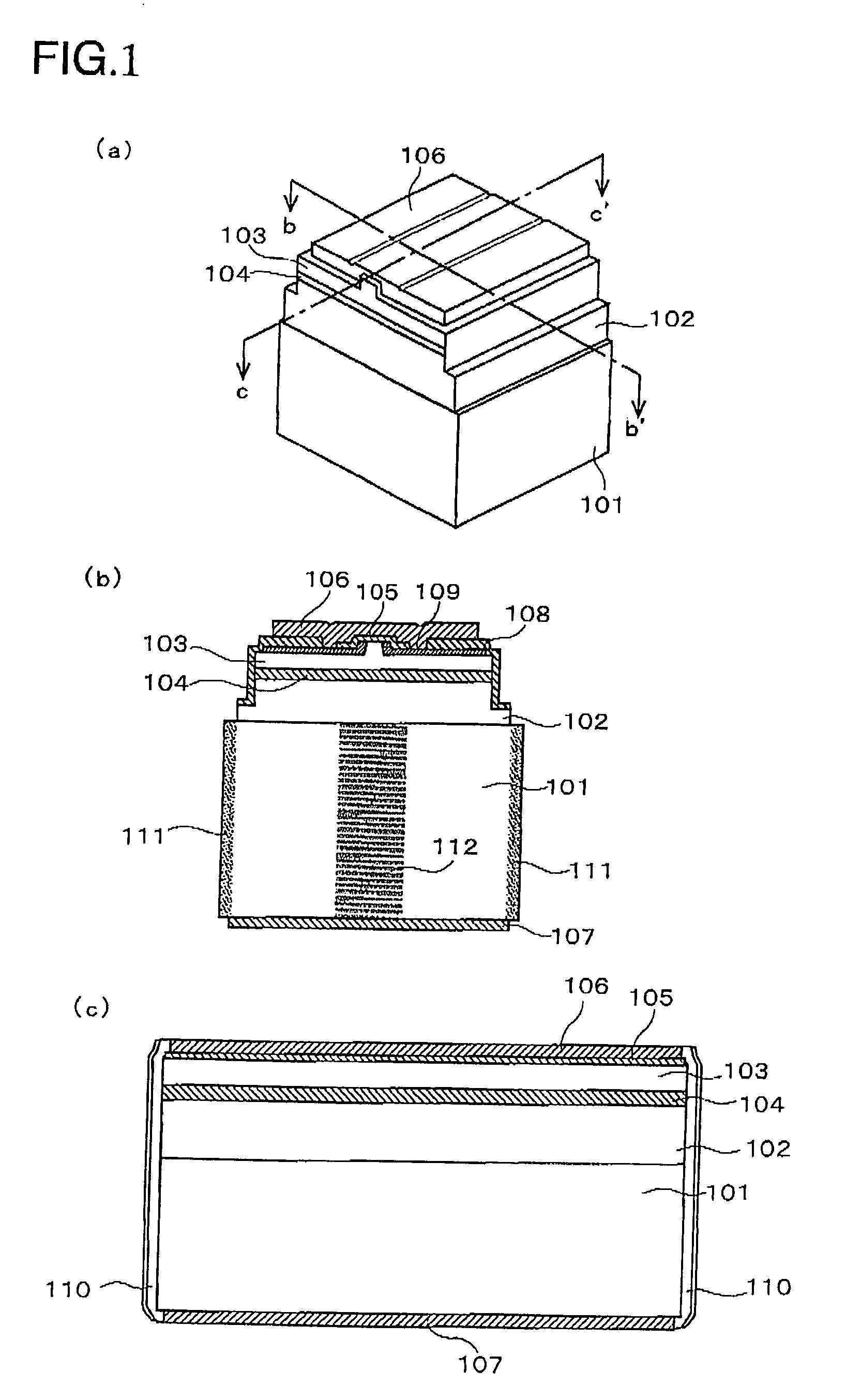
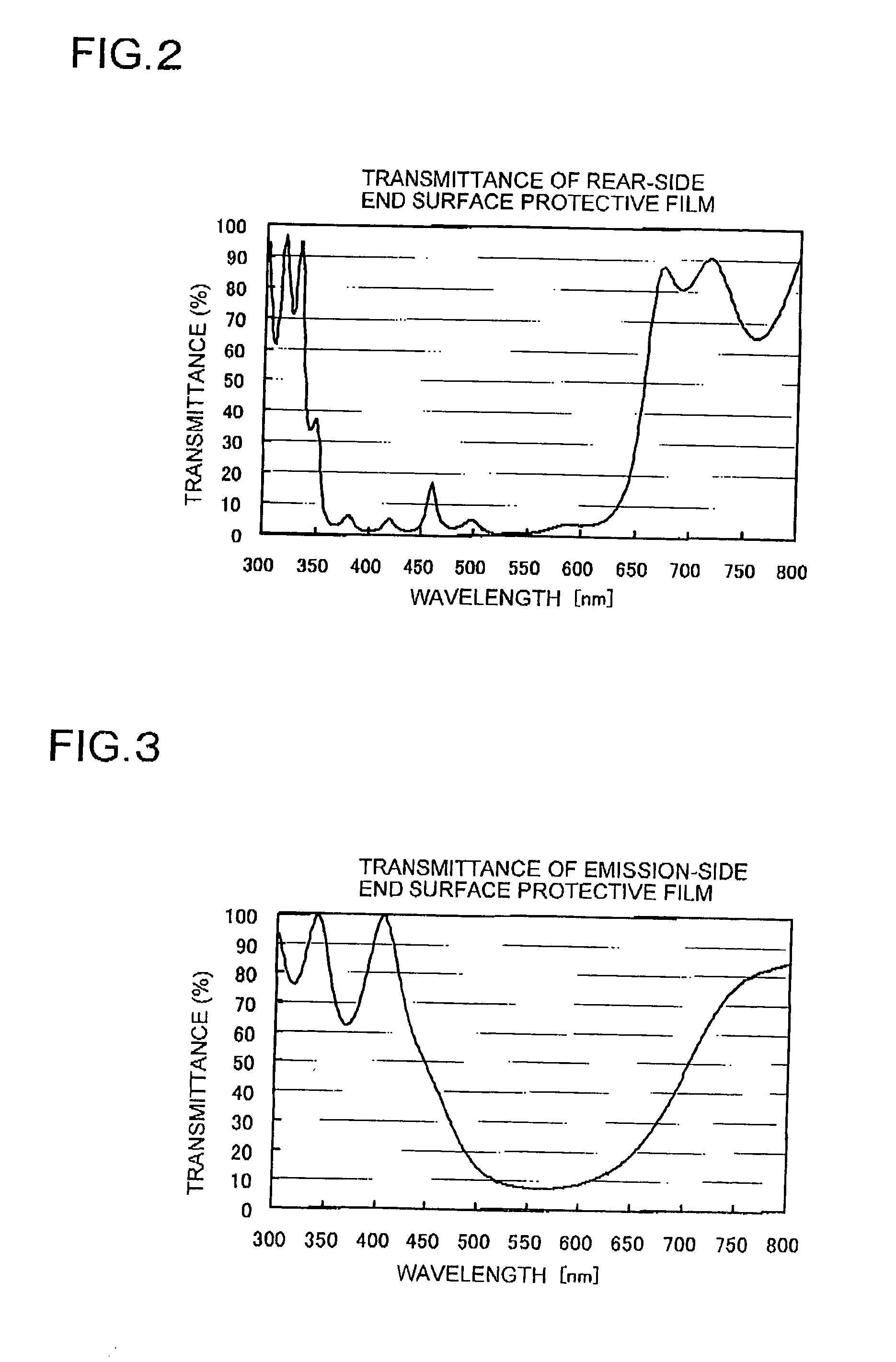
[0118] In an example 2, a third end surface protective film composed of Al2O3(1800 Å) / three pairs of (SiO2 (917 Å) / Nb2O5 (550 Å)) is provided on an emission side end surface. A second end surface protective film composed of ZrO2 (440 Å)+six pairs of (SiO2 (667 Å) / TiO2 (370 Å)) is provided on a rear side end surface. In addition, a first end surface protective film composed of ZrO2 (440 Å)+six pairs of (SiO2 (917 Å) / TiO2 (509 Å)) is provided thereon. Similarly to the example 1, in the case where the wavelength of light emitted from the active layer 104 is 400 nm, and the wavelength of luminescent radiation that is emitted by absorption of the wavelength of the light emitted from the active layer is 550 nm, as for the wavelengths (A), these thicknesses are set to λ / 4n (where n is the refractive index). In addition, an n-electrode 107 is provided on the back surface of the nitride semiconductor substrate. V / Pt / Au (150 Å / 2000 Å / 3300 Å) is provided as the material of the n-electrode. Aft...

example 3

[0119] In an example 3, a substrate that is obtained as follows is used as a nitride semiconductor substrate. A GaAs substrate is used as a growth substrate. A stripe-shaped protective layer of SiO2 is formed in parallel to the M-plane of a nitride semiconductor on the upper surface of the substrate. A nitride semiconductor is grown by using this as a seed crystal such that the facet surface appears. Thus, a nitride semiconductor substrate 101 with thickness of 300 μm is obtained. The nitride semiconductor substrate obtained as described above is a nitride semiconductor substrate has a stripe-shaped low dislocation density region and a dislocation flux region. A ridge is formed in the upper part of the low dislocation density region 112. The low dislocation density 112 region is a luminescent radiation region. It absorbs light emitted from the active layer (405 nm) when a current is applied, and emits luminescent radiation (560 nm). In the example 3, although the n-electrode 107 is ...


PUM


Abstract

A nitride semiconductor laser device comprises a nitride semiconductor substrate (101); a nitride semiconductor lamination structure that has an n-type semiconductor layer (102), an active layer (104) and a p-type semiconductor layer (103) laminated on or above the nitride semiconductor substrate (101), and has a stripe-shaped waveguide region for laser light; and end surface protective films (110) on the both end surfaces substantially perpendicular to the waveguide region. In the nitride semiconductor laser device, the nitride semiconductor substrate (101) has a luminescent radiation region (112) that absorbs light emitted from the active layer (104) and emits luminescent radiation with a wavelength longer than the wavelength of the emitted light, and the end surface protective films (110) have a high reflectivity for the wavelength of the luminescent radiation from the luminescent radiation region (112). Accordingly, a nitride semiconductor laser device that does not improperly operate and has excellent FFP is provided.

Description

BACKGROUND OF THE INVENTION [0001] 1. Technical Field [0002] The present invention relates a semiconductor laser device with a dielectric protective film formed on the end surface of a semiconductor layer using a nitride semiconductor, and more particularly to a high power semiconductor laser device using a nitride semiconductor substrate. A III-V group nitride semiconductor including GaN, AlN and InN, and a mixture crystal of them as AlGaN group, InGaN group and AlInGaN group can be given as the specific composition of the semiconductor device. [0003] 2. Description of Related Art [0004] Nitride semiconductor elements have light emission from the ultraviolet range in relatively short wavelength to the visible light range comprising red, and are widely used as materials that compose a semiconductor laser diode (LD), a light emitting diode (LED), and so on. In these years, they are getting to improve the miniaturization, life, reliability and output power, and are used mainly for lig...

Claims


Application Information

Patent Timeline
Patent Type & Authority Applications(United States)
IPC IPC(8): H01S5/00H01S3/04H01S5/028H01S5/20H01S5/323
CPCH01S5/028H01S5/32341H01S5/20
Inventor MATSUMURA, HIROAKIOCHIAI, MASANAO
Owner NICHIA CORP
Why Eureka
Try Eureka