Method for formng impurity-introduced layer, method for cleaning object to be processed apparatus for introducing impurity and method for producing device

a technology of impurity introduction and impurity processing, applied in mechanical devices, electrical control, machines/engines, etc., can solve the problems of metal contamination level, inability to improve the contamination level as good as the level of ion implantation

Active Publication Date: 2006-11-23
SAMSUNG ELECTRONICS CO LTD
View PDF15 Cites 85 Cited by
  • Summary
  • Abstract
  • Description
  • Claims
  • Application Information

AI Technical Summary

Benefits of technology

[0012] The present invention addresses the problems discussed above, and aims to provide a cleaning method that can clean a semiconductor substrate (solid substrate) such as a silicon substrate, in which impurity such as particles have been introduced. The

Problems solved by technology

After the introduction of particles, a level of metal contamination is a cause for concern, in particular, when the plasma doping is used because of the following reason: In the case of ion implantation, particles other than desired ones are removed by an analytical electromagnet; however, the plasma doping does not use the analytical electromagnet and exposes the silicon substrate directly to plasma.
In other words, the chamber inner wall is exposed to plasma, and the silicon substrate is exposed to the same plasma, so that metal contamination caused by the chamber tends to occur.
According to the foregoing reports, the concerns about the metal contamination can be solved at a research and development stage; however, the contamination level is not yet improved as good as that of the ion implantation.
The metal contamination is one of t

Method used


Image

  • Method for formng impurity-introduced layer, method for cleaning object to be processed apparatus for introducing impurity and method for producing device
  • Method for formng impurity-introduced layer, method for cleaning object to be processed apparatus for introducing impurity and method for producing device
  • Method for formng impurity-introduced layer, method for cleaning object to be processed apparatus for introducing impurity and method for producing device

Examples


embodiment 1

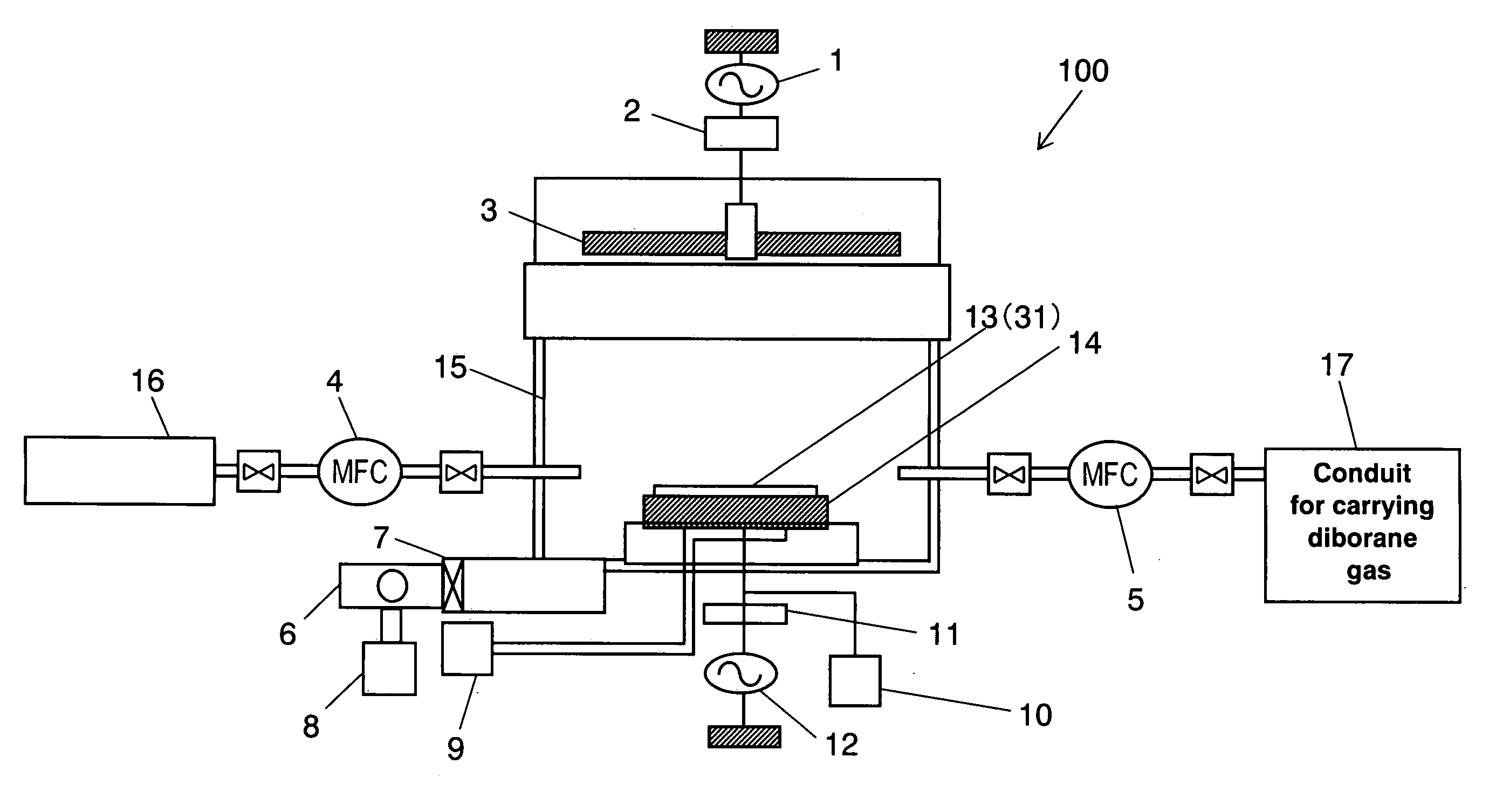
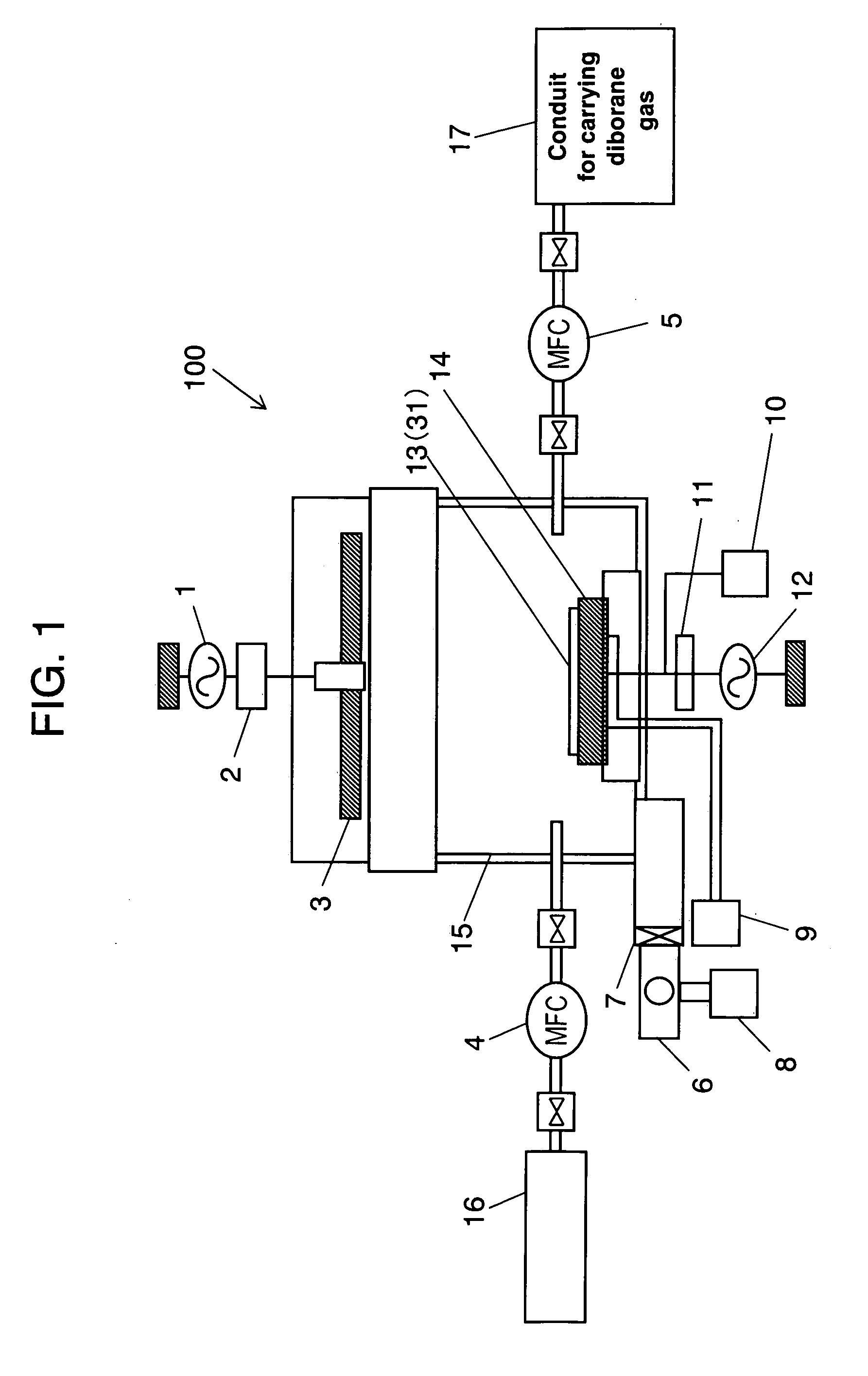
[0092]FIG. 10 shows a flowchart in accordance with the first embodiment of the present invention. FIG. 11A-FIG. 11C show a sectional view schematically illustrating an impurity-introduced layer which forms parts of a device, e.g. a transistor, built in silicon substrate 31, which is substantially the same as silicon substrate 13 used hitherto. The sectional views shown in FIG. 11A-FIG. 11C illustrate parts of electronic devices, i.e. structural elements such as diodes, resistors, capacitors or coils, schematically in a simple way.

[0093] The first embodiment is demonstrated hereinafter with reference to FIG. 10, FIG. 11A-FIG. 11C. As shown in FIG. 10, first, prepare silicon substrate 31, and form a resist on a principal face thereof, then conduct resist patterning S27 to etch a desirable resist pattern through a known etching process. FIG. 11A shows the completed state, namely, a given resist pattern 30 and opening 32 are formed on the principal face of substrate 31. Then plasma-dop...

embodiment 2

[0101]FIG. 12 shows a flowchart in accordance with the second embodiment of the present invention. The second embodiment differs from the first embodiment in resist removal S28a where SPM or APM are used. Other steps are similar to those of the first embodiment, so that the same reference marks are used.

[0102] The second embodiment is demonstrated hereinafter with reference to FIG. 10 and FIG. 12. A resist is formed on silicon substrate 31, and a desirable resist-patterning S27 is carried out, so that resist pattern 30 as well as opening 32 as shown in FIG. 11A is formed on a principal face of silicon substrate 31. Then plasma-doping S23 is carried out in the typical ion mode S23a. Before this plasma-doping S23, plasma irradiation for amorphization using rare gas, hydrogen or mixed gas thereof can be done. Opening 32 shown in FIG. 11A is exposed to the plasma used in the plasma irradiation and amorphization as well as the plasma used in the plasma-doping applied onto the principal ...

embodiment 3

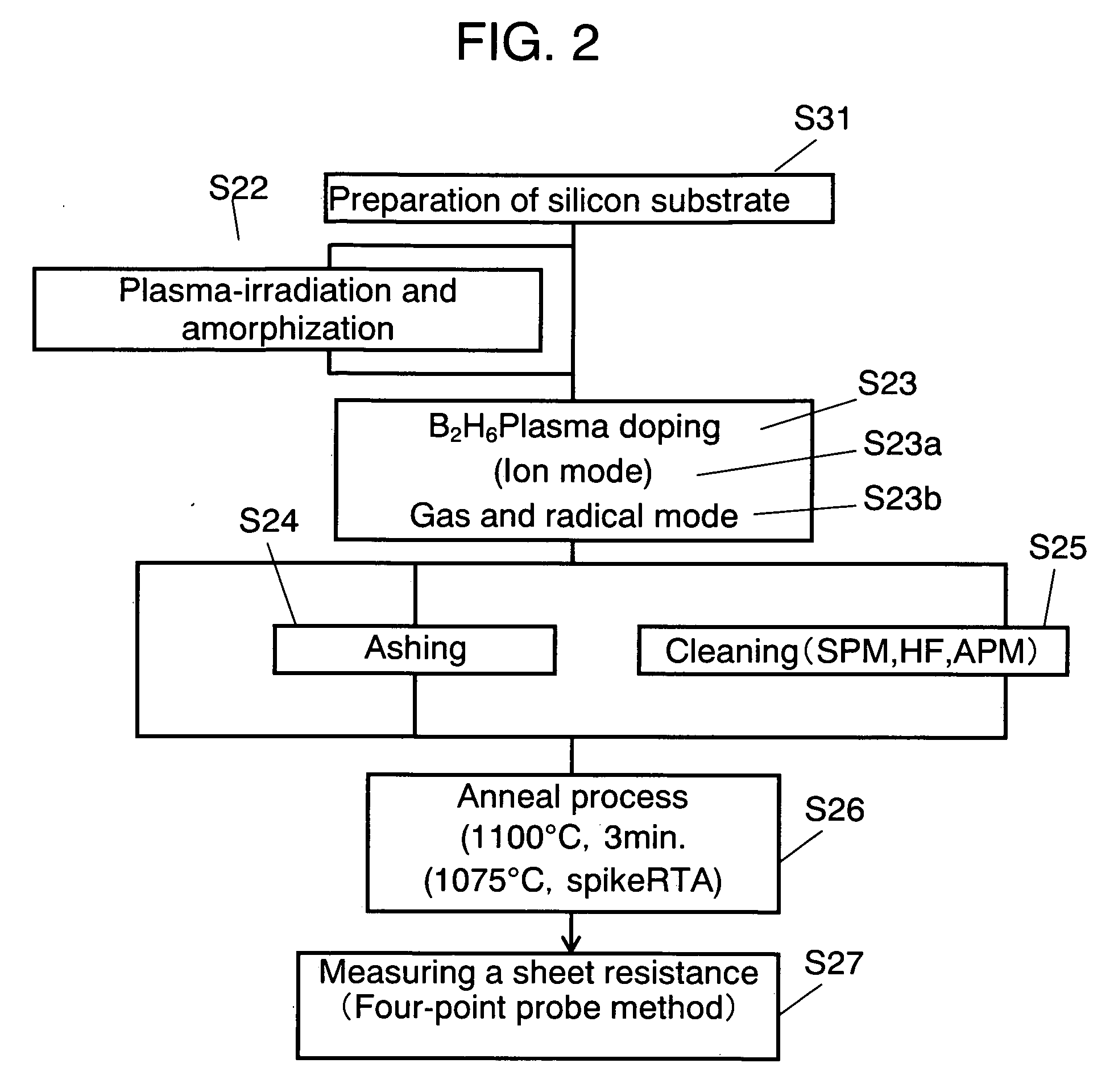
[0110]FIG. 13 shows a flowchart in accordance with the third embodiment of the present invention. This flowchart differs from the one shown in FIG. 10 in gas and radical mode S23b and also a little bit in the cleaning step.

[0111] The third embodiment is demonstrated hereinafter with reference to FIG. 13 and FIG. 11. As described in the first and the second embodiments, first, form a resist on silicon substrate 31, and etch a desirable resist pattern. FIG. 11A shows this status. Then irradiate substrate 31 with plasma of rare gas or hydrogen, or mixed-gas of those two gases for amorphization S22 before plasma-doping S23 in the typical gas and radical mode S23b.

[0112] Throug opening 32 of the resist shown in FIG. 11A, the principal face (surface) of silicon substrate 31 is exposed to the plasma used in plasma-irradiation and amorphization and the plasma used in plasma-doping S23. After the silicon is amorphizaed, boron is introduced and infiltrated into the silicon, so that impurity...


PUM

PropertyMeasurementUnit
Nanoscale particle sizeaaaaaaaaaa
Carrier concentrationaaaaaaaaaa

Abstract

A method of forming an impurity-introduced layer is disclosed. The method includes at least a step of forming a resist pattern on a principal face of a solid substrate such as a silicon substrate (S27); a step of introducing impurity into the solid substrate through plasma-doping in ion mode (S23), a step of removing a resist (S28), a step of cleaning metal contamination and particles attached to a surface of the solid substrate (S25a); a step of anneal (S26). The step of removing a resist (S28) irradiates the resist with oxygen-plasma or brings mixed solution of sulfuric acid and hydrogen peroxide water, or mixed solution of NH4OH, H2O2 and H2O into contact with the resist. The step of cleaning (S25a) brings mixed solution of sulfuric acid and hydrogen peroxide water, or mixed solution of NH4OH, H2O2 and H2O into contact with the principal face of the solid substrate. The step of removing a resist (S28) and the step of cleaning (S25a) can be conducted simultaneously by bringing mixed solution of sulfuric acid and hydrogen peroxide water, or mixed solution of NH4OH, H2O2 and H2O into contact with the principal face of the solid substrate.

Description

TECHNICAL FIELD [0001] The present invention relates to a method for introducing impurity into an object to be processed, thereby forming an impurity-introduced layer. To be more specific, the method is used in the process of manufacturing semi-conductors or liquid crystal, and introduces particles into an object to be processed, e.g. a silicon-substrate, through plasma-doping, ion-implantation, or deposition, thereby forming an impurity introduced layer. The present invention also relates to a method for cleaning the object such as the silicon substrate, and an impurity-introducing apparatus for providing the foregoing methods, and yet, the present invention relates to a method for manufacturing devices such as transistors, diodes, resistors and capacitors. BACKGROUND ART [0002] A conventional method of cleaning silicon substrates to be used as material of semiconductors has used hydrogen fluoride, mixed solution such as sulfuric acid and hydrogen peroxide water, mixed solution of ...

Claims


Application Information

Patent Timeline
IPC IPC(8): H01L21/302B08B6/00F01N11/00F02B37/18F02B39/16F02D23/00F02D41/00H01L21/02H01L21/223H01L21/265H01L21/304
CPCH01L21/2236H01L21/02052
Inventor THIBAUT, KEIN
Owner SAMSUNG ELECTRONICS CO LTD
Why Eureka
Try Eureka