Method to increase tensile stress of silicon nitride films using a post PECVD deposition UV cure

Active Publication Date: 2006-11-30
APPLIED MATERIALS INC
View PDF59 Cites 106 Cited by
  • Summary
  • Abstract
  • Description
  • Claims
  • Application Information

AI Technical Summary

Benefits of technology

[0008] An embodiment of a method in accordance with the present invention for forming silicon nitride, comprises, (i) disposing a workpiece including a surface in a processing chamber, (ii) depositing material on the surface by exposing the surface i

Problems solved by technology

However, such conventional methods face mounting problems as the size and spacing of the devices become ever smaller.
Similar benefits which are obtained from reducing gate dielectric thickness, such as decreased gate delay, are limited in small devices by

Method used


Image

  • Method to increase tensile stress of silicon nitride films using a post PECVD deposition UV cure
  • Method to increase tensile stress of silicon nitride films using a post PECVD deposition UV cure
  • Method to increase tensile stress of silicon nitride films using a post PECVD deposition UV cure

Examples


first embodiment

[0095] In accordance with the first embodiment just mentioned, a plasma pre-treatment step prior to deposition of silicon nitride in the presence of hydrogen can be employed. This pre-deposition plasma treatment cleans the wafer surface, removing contamination that could render the surface susceptible to penetration by hydrogen, such as residual silane or metallic contaminants such as Zn and Na. The plasma utilized for this pre-treatment step may be formed from a number of different ambients, including but not limited to N2O, O2 and NH3-containing plasmas which have been successfully used to reduce the number of defects of the nitride film post anneal. The pre treatment may be applied in the same or in a different processing chamber in which the SiN is deposited. The plasma treatment may conclude prior to the subsequent deposition step, or may be continuous and extend into the SiN deposition step. The specific parameters of this plasma pre-treatment, such as duration, power, tempera...

second embodiment

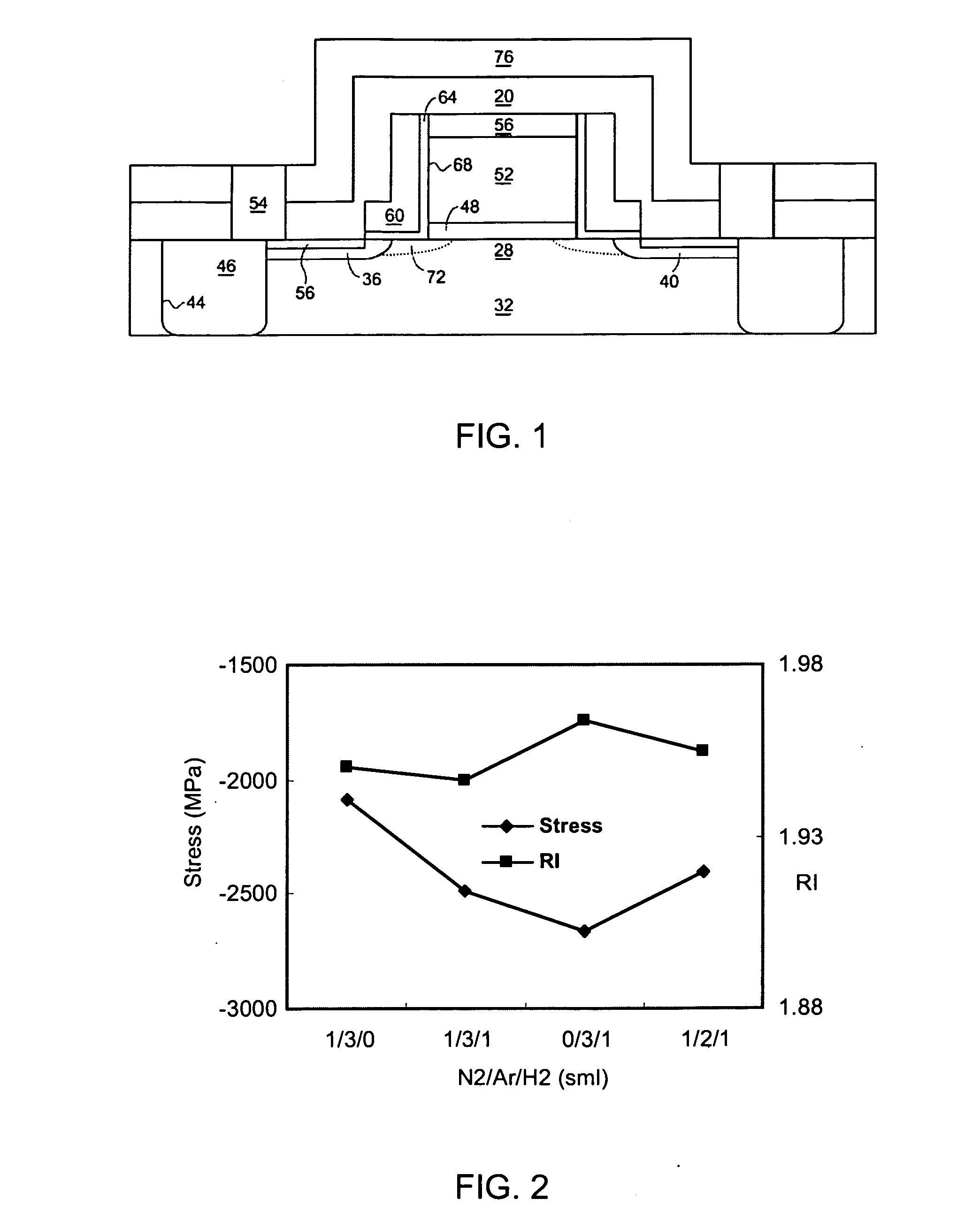
[0096] In accordance with the present invention mentioned above, defects can be reduced and reliability improved, by forming a buffer layer on the surface that is to receive the high compressive stress nitride. Such a buffer layer, typically comprising oxide, will then be located at the nitride / NiSix interface. This oxide serves as a buffer layer, blocking hydrogen diffusing through the deposited SiN film. Atomic hydrogen reaching the oxide buffer will attempt to combine with other hydrogen atoms to form molecular hydrogen, but will be unsuccessful in doing so owing to the strength of the Si—N, Si—H, and N—H bonds. Specifically, hydrogen diffuses by hopping from one Si—H or N—H bond to another. To migrate out of the nitride layer into the oxide layer, and Si—O bond needs to break and an Si—N bond will form. This reaction id not energetically favorable, so the hydrogen will remain trapped in the nitride layer. In this manner, the oxide buffer layer acts as a wall, preventing gas accu...


PUM

PropertyMeasurementUnit
Temperatureaaaaaaaaaa
Fractionaaaaaaaaaa
Pressureaaaaaaaaaa

Abstract

High tensile stress in a deposited layer such as silicon nitride, may be achieved utilizing one or more techniques, employed alone or in combination. High tensile stress may be achieved by forming a silicon-containing layer on a surface by exposing the surface to a silicon-containing precursor gas in the absence of a plasma, forming silicon nitride by exposing said silicon-containing layer to a nitrogen-containing plasma, and then repeating these steps to increase a thickness of the silicon nitride created thereby. High tensile stress may also be achieved by exposing a surface to a silicon-containing precursor gas in a first nitrogen-containing plasma, treating the material with a second nitrogen-containing plasma, and then repeating these steps to increase a thickness of the silicon nitride formed thereby. In another embodiment, tensile film stress is enhanced by deposition with porogens that are liberated upon subsequent exposure to UV radiation or plasma treatment.

Description

CROSS-REFERENCE TO RELATED APPLICATION [0001] This instant nonprovisional application is related to commonly assigned U.S. patent application Ser. No. 60 / 685,365, filed on May 26, 2005 and U.S. patent application Ser. No. 60 / 701,854, filed on Jul. 21, 2005, the entire disclosure of which is incorporated herein by reference.BACKGROUND OF THE INVENTION [0002] In the processing of a substrate to fabricate circuits and displays, the substrate is typically exposed to an energized process gas capable of depositing or etching material on the substrate. In chemical vapor deposition (CVD) processes, process gas energized by a high frequency voltage or microwave energy is used to deposit material on the substrate, which may be a layer, a filling of contact holes, or other selective deposition structures. The deposited layer can be etched or otherwise processed to form active and passive devices on the substrate, such as for example, metal-oxide-semiconductor field effect transistors (MOSFETs)...

Claims


Application Information

Patent Timeline
IPC IPC(8): H05H1/24B05D3/00
CPCC23C16/345C23C16/45523C23C16/56H01L21/3141H01L21/823835H01L21/823412H01L21/82345H01L21/823807H01L21/3185H01L21/0217H01L21/02274H01L21/0234H01L21/02348H01L21/02216H01L21/324
Inventor BALSEANU, MIHAELACOX, MICHAEL S.XIA, LI-QUNSHEK, MEI-YEELEE, JIAZUBKOV, VLADIMIRHUANG, TZU-FANGWANG, RONGPINGROFLOX, ISABELITAM'SAAD, HICHEM
Owner APPLIED MATERIALS INC
Why Eureka
Try Eureka