Vacuum reaction chamber with x-lamp heater

a technology of vacuum reaction chamber and x-lamp heater, which is applied in the field of vacuum reaction chamber with x-lamp heater, can solve the problems of negative side effects of current electron beam chamber design on a substrate, damage or destruction of semiconductor devices, and the design of current electron beam chamber can have negative side effects on a substrate, so as to reduce the damage to the substrate

Inactive Publication Date: 2006-12-07
APPLIED MATERIALS INC
View PDF10 Cites 14 Cited by
  • Summary
  • Abstract
  • Description
  • Claims
  • Application Information

AI Technical Summary

Benefits of technology

[0011] Embodiments of the invention provide an electron beam apparatus for processing a substrate. In one embodiment, the electron beam apparatus for processing a substrate comprises a vacuum chamber. The vacuum chamber comprises an electron source. The electron source comprises an anode, a low voltage source connected to the anode, a cathode, and a high voltage source connected to the cathode. The vacuum chamber further comprises a substrate support and a grid configured to reduce damage to the substrate during electron beam treatment, wherein the gird is located between the anode and the substrate support. A bias source is connected to the grid. In one embodiment, the vacuum chamber further comprises a cross lamp heating device. In another embodiment, the vacuum chamber further comprises at least one thermocouple assembly. In another embodiment the thermocouple assembly comprises a resilient member made of ceramic material. In another embodiment the ceramic material is selected for a group consisting of silicon carbide, silicon nitride, aluminum nitride, synthetic diamond and combinations thereof.
[0012] In another embodiment, a method of reducing charging damage to a substrate during electron beam treatment is provided. The method comprises providing a chamber comprising a grid located between an anode and a substrate support and applying a bias voltage to the grid, wherein the bias voltage is provided at conditions sufficient to fully or partially neutralize the electron beam charge on the substrate. In one embodiment, the conditions are sufficient to reduce the substrate charge current to less than about 0.005 mA. In one embodiment, the bias voltage is a DC bias. In another, the bias voltage is a RF bias. In another embodiment, the substrate comprises a low dielectric constant film, and electron beam treatment of the low dielectric constant film comprises forming voids in the low dielectric constant film. In one embodiment the bias voltage is between about 3 V and about 40 V. In another embodiment, the bias voltage is between about −3 V and about −30 V.

Problems solved by technology

However, current electron beam chamber designs suffer from several major drawbacks.
First, current electron beam chamber designs can have negative side effects on a substrate, such as damage or destruction of semiconductor devices on a substrate.
It is believed that the electron beam treatment damages substrates by causing an excess negative charge build up on the substrates from the electrons bombarding the substrate.
The excess negative charge build up during device manufacturing can create charge currents that form undesirable current paths in areas of the substrate that are normally insulating, and leakage current through the newly created current paths during operation of the devices can destroy the devices on the substrate.
Second, current electron beam chamber designs have contributed to heavy metal contamination of substrates.
Third, poor within substrate shrinkage due to a lack of temperature uniformity across the substrate surface has been exhibited.

Method used


Image

  • Vacuum reaction chamber with x-lamp heater
  • Vacuum reaction chamber with x-lamp heater
  • Vacuum reaction chamber with x-lamp heater

Examples


example 1

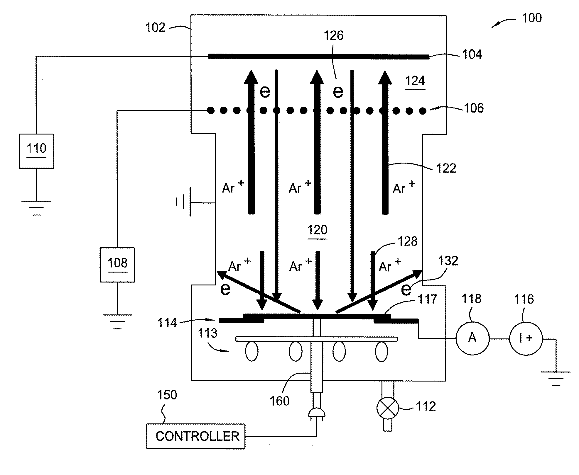
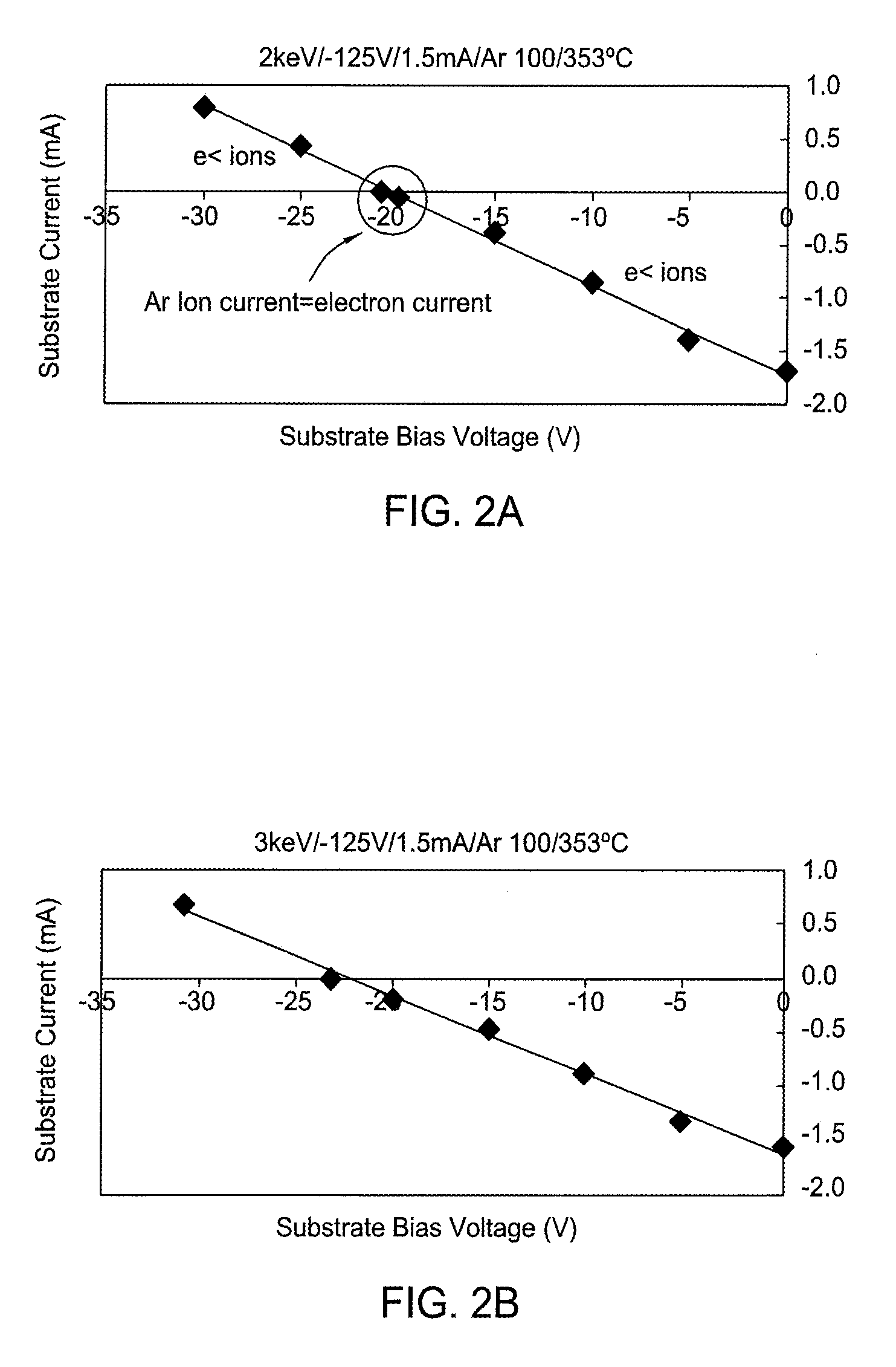
[0058] A bare silicon substrate was electron beam treated an apparatus as shown in FIG. 1 under the following conditions: an electron beam energy of 2 keV, an anode voltage of −125 V, an electron beam current of 1.5 mA, an argon flow of 100 sccm, and a substrate temperature of 353° C. The charge current on the substrate was measured at different substrate DC bias voltages. FIG. 2A is a graph showing the charge current on the substrate at different substrate DC bias voltages.

example 2

[0059] A bare silicon substrate was electron beam treated under the following conditions: an electron beam energy of 3 keV, an anode voltage of −125 V, an electron beam current of 1.5 mA, an argon flow of 100 sccm, and a substrate temperature of 353° C. The charge current on the substrate was measured at different substrate DC bias voltages. FIG. 2B is a graph showing the charge current on the substrate at different substrate DC bias voltages.

[0060]FIG. 2A shows that a substrate charge current of 0 mA or about 0 mA was obtained when a substrate bias voltage of approximately −20 V was applied to the substrate during an electron beam treatment having an energy of 2 keV. FIG. 2B shows that a substrate charge current of 0 mA or about 0 mA was obtained when a substrate bias voltage of approximately −23 V was applied to the substrate during an electron beam treatment having an energy of 3 keV. Thus, FIGS. 2A and 2B illustrate that embodiments of the invention provide a method of producin...

example 3

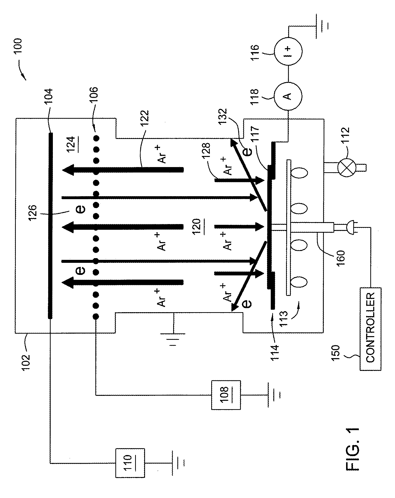
[0063] Silicon substrates having a film of Black Diamond IIx (process conditions available from Applied Materials, Inc. of Santa Clara, Calif.) deposited thereon were electron beam treated in an apparatus as shown in FIG. 3 under the following conditions: an electron beam energy of 3.3 keV, an anode voltage of −125 V, an electron beam current of 1.5 mA, an argon flow of 100 sccm, and a substrate temperature of 400° C. The grounded aluminum wire grid of the apparatus had 66% transparency, a wire diameter of 10 mils, and 0.011 inch diameter openings. The charge current on the substrates was measured at different grid bias voltages. The charge current on the substrates increased as the grid bias voltage was increased and reached 0 at a grid bias voltage of 25 V. The properties, including thickness, refractive index, shrinkage, thickness uniformity, dielectric constant, and stress, of the Black Diamond IIx films after the electron beam treatments were comparable to the properties of Bla...


PUM

PropertyMeasurementUnit
charge currentaaaaaaaaaa
bias voltageaaaaaaaaaa

Abstract

Methods and apparatus for electron beam treatment of a substrate are provided. An electron beam apparatus that includes a vacuum chamber, at least one thermocouple assembly in communication with the vacuum chamber, a heating device in communication with the vacuum chamber, and combinations thereof are provided. In one embodiment, the vacuum chamber comprises an electron source wherein the electron source comprises a cathode connected to a high voltage source, an anode connected to a low voltage source, and a substrate support. In another embodiment, the vacuum chamber comprises a grid located between the anode and the substrate support. In one embodiment the heating device comprises a first parallel light array and a second light array positioned such that the first parallel light array and the second light array intersect. In one embodiment the thermocouple assembly comprises a temperature sensor made of aluminum nitride.

Description

CROSS-REFERENCE TO RELATED APPLICATIONS [0001] This application is a continuation-in-part of co-pending U.S. patent application Ser. No. 11 / 383,383 (APPM / 009914.P1), filed May 15, 2006, which is a continuation-in-part of co-pending U.S. patent application Ser. No. 11 / 143,270 (APPM / 009914), filed Jun. 2, 2005. This application also claims benefit of United States provisional patent application Ser. No. 60 / 717,386 (APPM / 010221L), filed Sep. 15, 2005; and benefit of United States provisional patent application Ser. No. 60 / 781,908 (APPM / 010221L02), filed Mar. 13, 2006. Each of the aforementioned related patent applications is herein incorporated by reference.BACKGROUND OF THE INVENTION [0002] 1. Field of the Invention [0003] Embodiments of the present invention generally relate to the fabrication of integrated circuits. More particularly, embodiments of the present invention relate to an apparatus and method for electron beam treatment of a substrate. [0004] 2. Description of the Relate...

Claims


Application Information

Patent Timeline
Patent Type & Authority Applications(United States)
IPC IPC(8): C23F1/00B44C1/22
CPCB23K15/00C23F4/00H01J37/026H01J37/20H01J37/317H01J2237/004H01L21/67115H01J2237/2001H01J2237/304H01J2237/3156H01J2237/316H01J2237/3165H01J2237/0044
Inventor AL-BAYATI, AMIRD'CRUZ, LESTER A.DEMOS, ALEXANDROS T.DUBOIS, DALE R.ELSHEREF, KHALED A.IWASAKI, NAOYUKIM'SAAD, HICHEMROCHA-ALVAREZ, JUAN CARLOSSHAH, ASHISHSHIMIZU, TAKASHI
Owner APPLIED MATERIALS INC
Why Eureka
Try Eureka