

Field-effect transistor and method for fabricating the same
a field-effect transistor and transistor technology, applied in semiconductor/solid-state device manufacturing, semiconductor devices, electrical equipment, etc., can solve the problems of difficult to obtain a large current density, and achieve the effect of reducing source resistance and drain resistance, reducing drain current, and small ga
- Summary
- Abstract
- Description
- Claims
- Application Information
AI Technical Summary
Benefits of technology
Problems solved by technology
Method used
Image

Examples
first embodiment
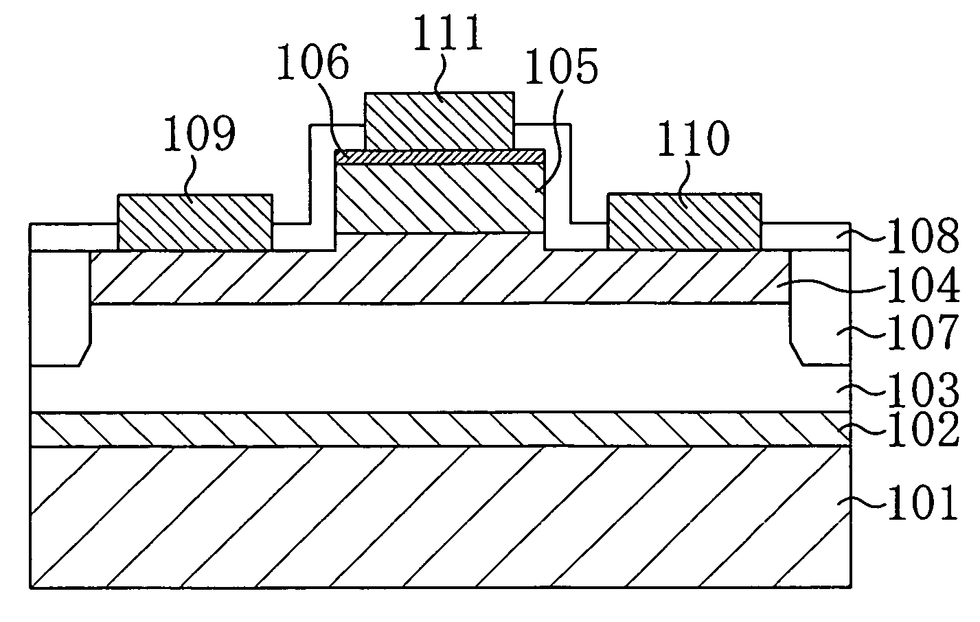
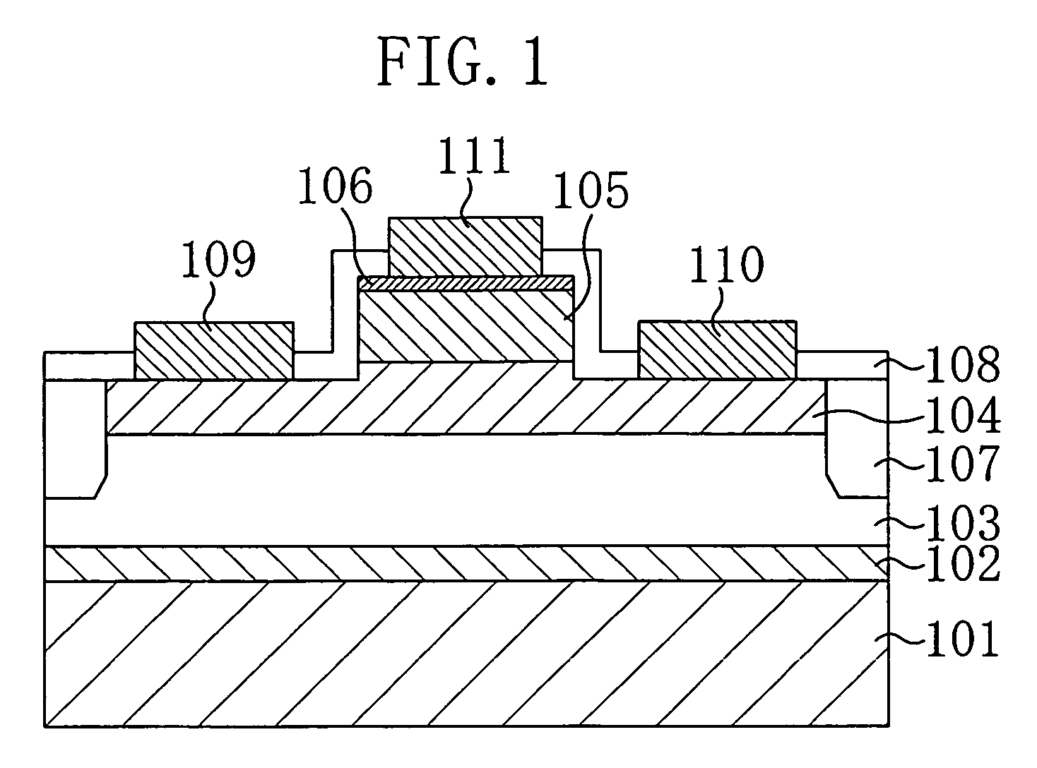
[0032]FIG. 1 is a cross-sectional view of a field-effect transistor according to a first embodiment of the present invention.
[0033] As shown in FIG. 1, the field-effect transistor of this embodiment includes a sapphire substrate 101, an AlN buffer layer 102 formed on the sapphire substrate 101 so as to have a thickness of 100 nm, an undoped GaN layer 103 formed on the AlN buffer layer 102 so as to have a thickness of 2 μm, an undoped AlGaN layer 104 formed on the undoped GaN layer 103 so as to have a thickness of 25 nm, a p-type GaN layer 105 formed on part of the undoped AlGaN layer 104 so as to have a thickness of 100 nm, and a heavily doped p-type GaN layer 106 formed on the p-type GaN layer 105 so as to contain a p-type impurity at a higher concentration than that of the p-type GaN layer 105 and have a thickness of 5 nm. Herein, “undoped” means a state in which an impurity is not intentionally doped. In the field-effect transistor of this embodiment, the undoped AlGaN layer 104...
second embodiment
[0047]FIG. 4 is a cross-sectional view of a field-effect transistor according to a second embodiment of the present invention.
[0048] As shown in FIG. 4, the field-effect transistor of this embodiment includes a sapphire substrate 401, an AlN buffer layer 402 formed on the sapphire substrate 401 so as to have a thickness of 100 nm, an undoped GaN layer 403 formed of the AlN buffer layer 402 so as to have a thickness of 2 μm, an undoped AlGaN layer 404 formed on the undoped GaN layer 403 so as to have a thickness of 25 nm, a p-type AlGaN layer 405 formed on part of the undoped AlGaN layer 404 so as to have a thickness of 100 nm, and a heavily doped p-type GaN layer 406 formed on the p-type AlGaN layer 405 so as to have a thickness of 5 nm. The field-effect transistor of this embodiment further includes a gate electrode 411 formed of Pd which forms an Ohmic contact with the heavily doped p-type GaN layer 406, a source electrode 409 and a drain electrode 410 each of which forms an Ohmi...
third embodiment
[0062]FIG. 9 is a cross-sectional view of a field-effect transistor according to a third embodiment of the present invention.
[0063] As shown in FIG. 9, the field-effect transistor of this embodiment includes a sapphire substrate 901, an AlN buffer layer 902 formed on the sapphire substrate 901 so as. to have a thickness of 100 nm, an undoped GaN layer 903 formed on the AlN buffer layer 902 so as to have a thickness of 2 μm, an n-type GaN layer 904 formed on the undoped GaN layer 903 so as to have a thickness of 5 nm, an undoped AlGaN layer 905 formed on the n-type GaN layer 904 so as to have a thickness of 20 nm, a p-type AlGaN layer 906 formed on the undoped AlGaN layer 905 so as to have a thickness of 100 nm, and a heavily doped p-type GaN layer 907 formed on the p-type AlGaN layer 906 so as to have a thickness of 5 nm. The field-effect transistor of this embodiment further includes heavily doped n-type regions 909 defined in parts located at both sides of the n-type GaN layer 90...
PUM
 Abstract
Description
Claims
Application Information