Method for forming via-hole in semiconductor device

a semiconductor device and via-hole technology, applied in semiconductor devices, semiconductor/solid-state device details, electrical apparatus, etc., can solve the problems of inability to manufacture large-scale commercial production of complex functional circuit devices, poor step coverage of vertical type of via-hole during metal deposition process, and inability to meet the gap-filling properties of via-hole and/or metal deposition method,

Inactive Publication Date: 2006-12-07
DONGBU ELECTRONICS CO LTD
View PDF9 Cites 8 Cited by
  • Summary
  • Abstract
  • Description
  • Claims
  • Application Information

AI Technical Summary

Benefits of technology

[0010] It is, therefore, an object of the present invention to provide a method for forming a via-hole to have a round top profile, thus enabling and / or facilitating filling the via-hole with a conductive material for interconnection of multilevel metallization and / or wiring.

Problems solved by technology

Multilevel interconnection technology is necessary to reduce the length of signal lines, thus enabling complicated functional circuit devices having a lower connection resistance and / or signal propagation time.
Here, a vertical type of via-hole generally has poor step coverage during the metal deposition process (i.e., the gap-fill properties of the via-hole and / or metal deposition method may be unacceptable for large-scale commercial production).
As a result, it becomes more difficult to completely fill a via-hole with CVD-W or CVD-Al.

Method used


Image

  • Method for forming via-hole in semiconductor device
  • Method for forming via-hole in semiconductor device
  • Method for forming via-hole in semiconductor device

Examples


Embodiment Construction

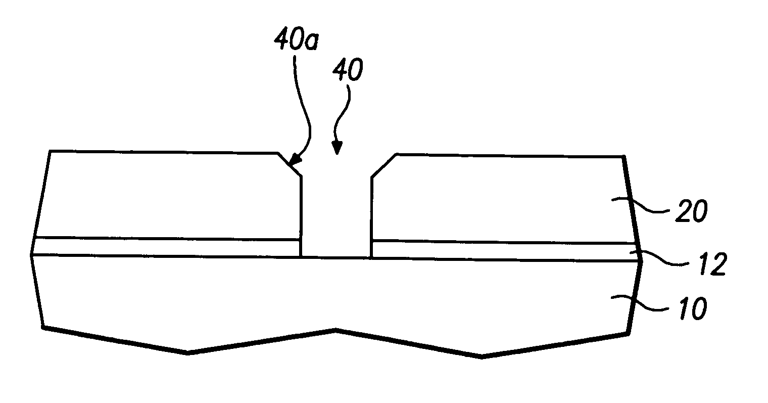
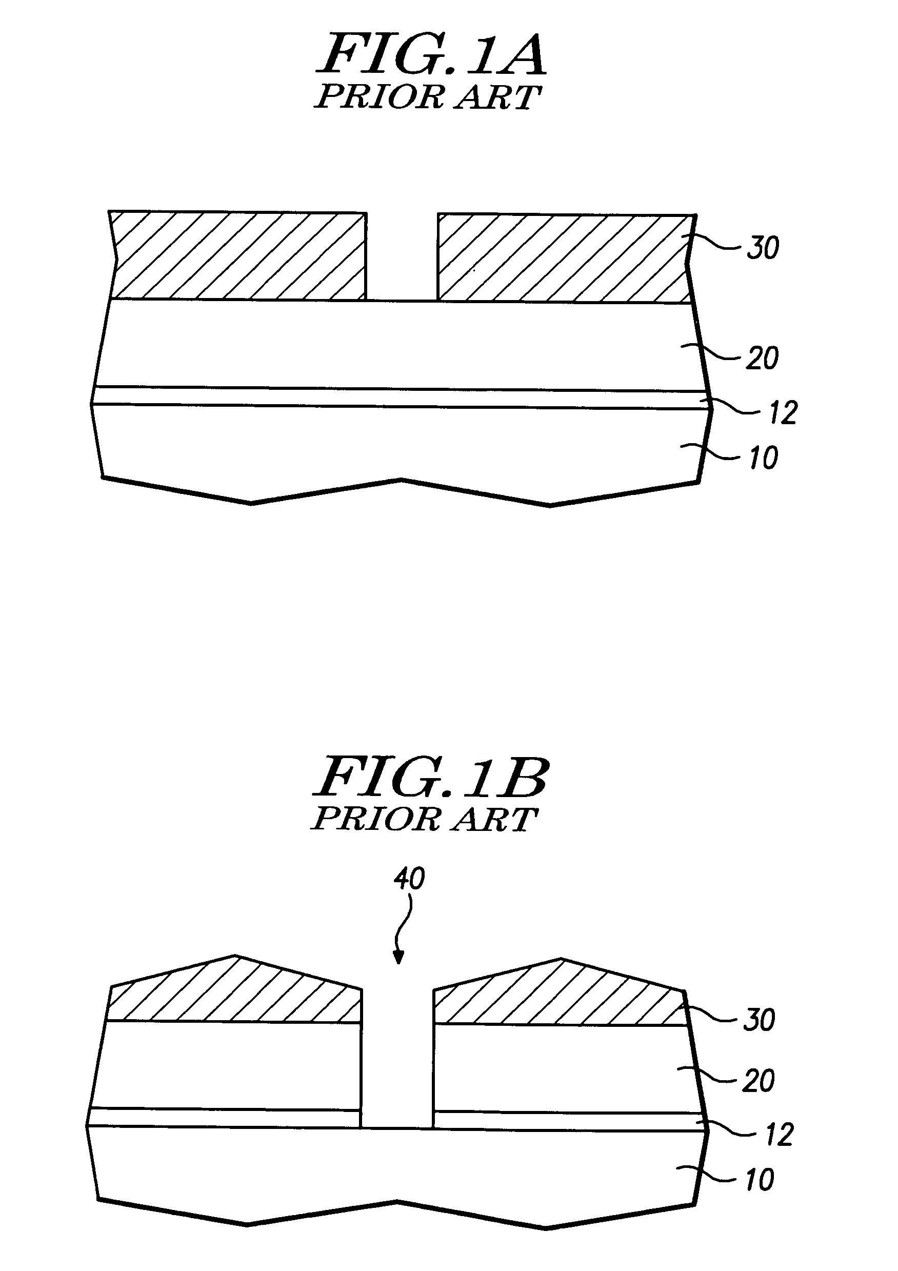
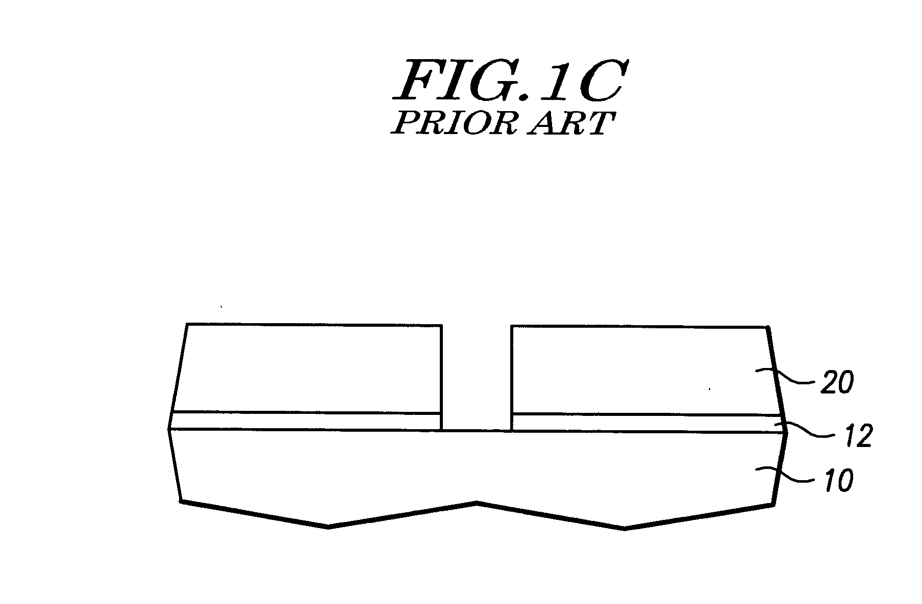
[0018] Referring to FIG. 2A, lower metallization layer 10 is formed on a semiconductor substrate (not shown), and a diffusion barrier layer 12 such as Ti and / or TiN (preferably a Ti layer with a TiN layer thereon) is formed thereon. Next, an insulating layer 20 such as an IMD is formed over an entire surface of the substrate, for the purpose of insulating metallization. The insulating layer 20 may comprise one or more layers of a silicon oxide, such as silicon dioxide (which may be optionally doped with fluorine, boron, phosphorous, or a mixture of boron and phosphorous), silicon nitride, silicon oxynitride, silicon-rich oxide, etc. In one embodiment, insulating layer 20 comprises a lower silicon nitride or silicon-rich oxide layer, with one or more layers of a (doped) silicon dioxide thereon. In one example, the (doped) silicon dioxide comprises a bulk layer of fluorosilicate glass (FSG) with layers of undoped silicate glass (USG) above and below the FSG layer. Then, a mask (e.g., ...


PUM

PropertyMeasurementUnit
pressureaaaaaaaaaa
pressureaaaaaaaaaa
poweraaaaaaaaaa

Abstract

Disclosed is a method for forming a via-hole for interconnection of metallization and/or metal wires in a semiconductor device. The present method may include the steps of: (a) forming an insulating layer on a semiconductor substrate including a lower metallization and/or metal wiring; (b) forming a mask (e.g., a photo-resist pattern) on the insulating layer; (c) dry etching the insulating layer using the photo-resist pattern as a mask to form a via-hole in the insulating layer; and (d) in the same dry etching chamber, etching a top portion of the insulating layer in the vicinity of the via-hole with an etchant comprising oxygen and argon.

Description

[0001] This application claims the benefit of Korean Application No. 10-2005-0047661, filed on Jun. 3, 2005, which is incorporated by reference herein in its entirety. BACKGROUND OF THE INVENTION [0002] 1. Field of the Invention [0003] The present invention relates to semiconductor device manufacturing technology, more specifically, to a method for forming a via-hole for interconnection between multilevel metallization and / or wiring layers. [0004] 2. Description of the Related Art [0005] Improvement in the integration of a semiconductor chip produces or results in decreasing the size of circuit elements, and also increasing the length of signal lines for electrical connection between elements, because a plurality of complicated functional elements are integrated on a single chip. However, the length of a signal line should be shortened to improve an operational speed of the integrated circuit. Multilevel interconnection technology is necessary to reduce the length of signal lines, t...

Claims


Application Information

Patent Timeline
Patent Type & Authority Applications(United States)
IPC IPC(8): H01L21/4763
CPCH01L21/02063H01L21/76804H01L21/31116H01L21/28H01L21/768
Inventor NAM, SANG WOO
Owner DONGBU ELECTRONICS CO LTD
Why Eureka
Try Eureka