Light transmitting substrate with transparent conductive film

Inactive Publication Date: 2006-12-21
NIPPON SODA CO LTD
View PDF4 Cites 15 Cited by
  • Summary
  • Abstract
  • Description
  • Claims
  • Application Information

AI Technical Summary

Benefits of technology

[0028] Examples of the transparent conductive film include films made of tin-doped indium oxide (ITO), zinc-doped indium oxide (IZO), aluminum-doped zinc oxide, FTO, ATO, ZnO, SnO2 and In2O3, and an ITO film is preferable. In case of increasing the light transmittance, the thinner the transparent conductive film, the better. Since it is necessary to form a continuous film having no island structure, the thickness of the film is from 12 to 2 nm, and preferably from 10 to 2 nm. The thickness of the film is preferably from 9 to 2 nm so as to increase the light transmittance, and is preferably from 8 to 2 nm so as to further increase the light transmittance. Regarding the light transmittance of the light transmitting substrate with a transparent conductive film of the present invention, the light transmittance to light having a wavelength of 400 nm is preferably 88% or more, more preferably 90% or more,

Problems solved by technology

Although a high-transparent light transmitting substrate with a transparent conductive film is required, the ITO film described in the publications described above is not sufficiently high-transparent, necessarily, within a visible range (

Method used


Image

  • Light transmitting substrate with transparent conductive film
  • Light transmitting substrate with transparent conductive film
  • Light transmitting substrate with transparent conductive film

Examples


Example

EXAMPLE 1

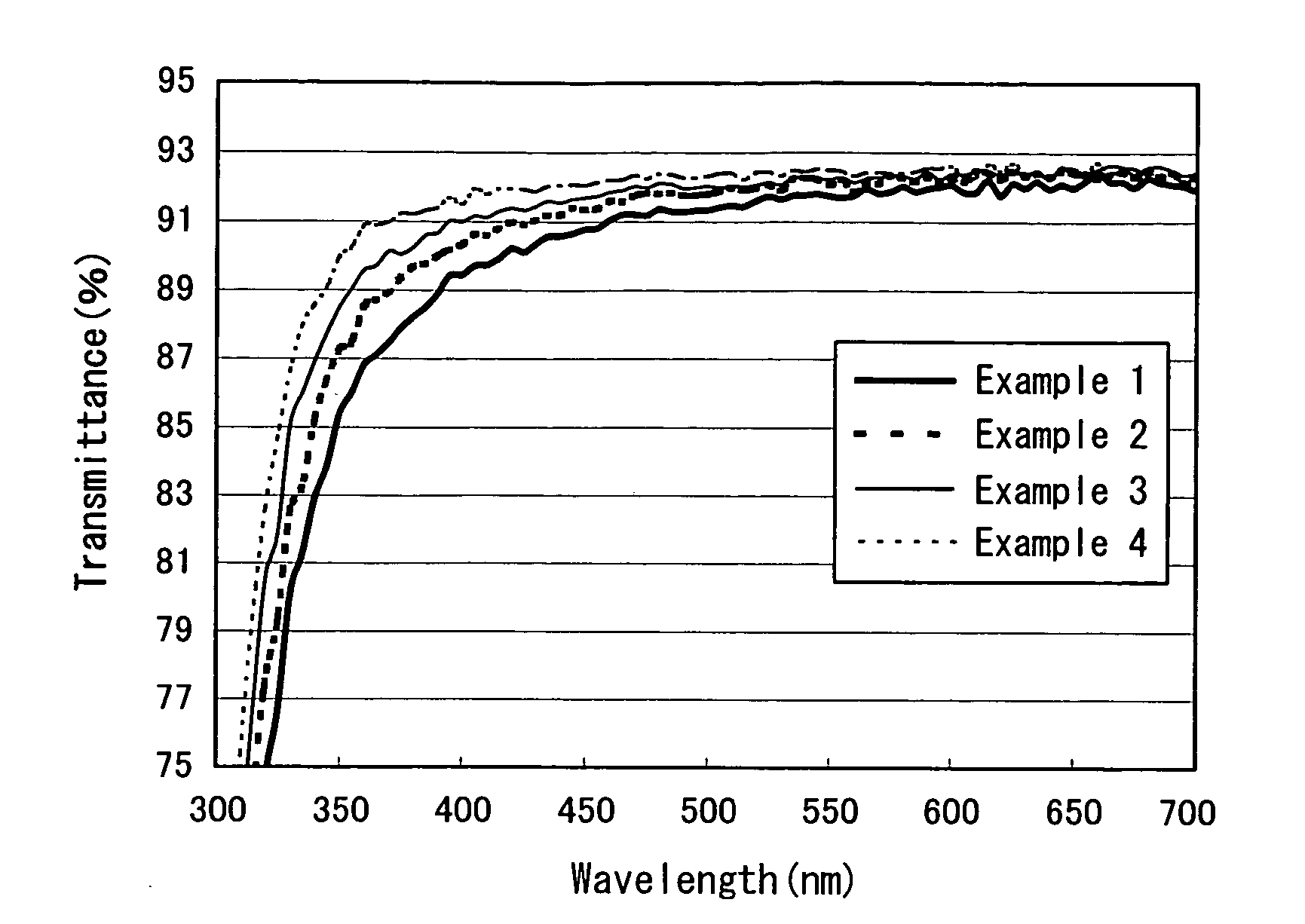
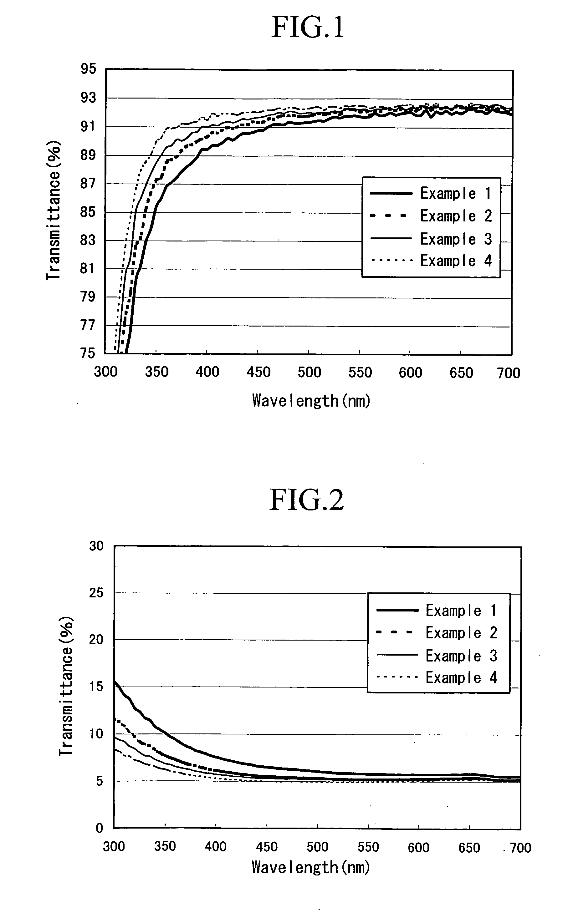
[0049] An ITO film was formed on a glass substrate by a pyrosol method. That is, a borosicilic acid (BLC) glass polished substrate (260×220×0.4 mm) precoated with a SiO2 film (thickness: 10 nm) was placed in a conveyer furnace heated to 500° C. through a belt conveyor and an acetylacetone solution of stannic chloride-indium acetylacetonate containing 12 atomic % of tin atoms was brown into the conveyer furnace using an air as a carrier gas after forming into fog drip, thereby to contact with the surface of the glass substrate and to cause thermal decomposition, and thus an ITO film having a thickness of 12 nm was formed. The resulting ITO film had a surface resistance value of 1.7 KΩ / □. The surface of the film was observed by an atomic force microscope (AFM). As a result, an average surface roughness Ra was 0.7 nm and a maximum surface roughness Rmax was 12 nm. A light transmittance of spectral characteristics of the resulting ITO glass is shown in FIG. 1 and a reflectance...

Example

EXAMPLE 2

[0050] In the same manner as in Example 1, except that the belt conveyor speed and the amount of the chemical to be atomized were adjusted, an ITO film having a thickness of 10 nm was formed.

[0051] The analytical results of the resulting ITO glass are shown in Table 1, a light transmittance of spectral characteristics are shown in FIG. 1, and a reflectance is shown in FIG. 2.

Example

EXAMPLE 3

[0052] An ITO film was formed on a glass substrate by a pyrosol method. That is, a borosicilic acid (BLC) glass polished substrate (260×220×0.4 mm) precoated with a SiO2 film (thickness: 10 nm) was placed in a conveyer furnace heated to 500° C. through a belt conveyor and an acetylacetone solution of stannic chloride-indium acetylacetonate containing 12 atomic % of tin atoms was brown into the conveyer furnace using an air as a carrier gas after forming into fog drip, thereby to contact with the surface of the glass substrate and to cause thermal decomposition, and thus an ITO film having a thickness of 8 nm was formed. The surface of the film was observed by AFM. As a result, an average surface roughness Ra was 0.8 nm and a maximum surface roughness Rmax was 13 nm. A light transmittance of spectral characteristics of the resulting ITO glass is shown in FIG. 1 and a reflectance is shown in FIG. 2.


PUM

PropertyMeasurementUnit
Temperatureaaaaaaaaaa
Fractionaaaaaaaaaa
Transparencyaaaaaaaaaa

Abstract

A sufficiently high-transparent light transmitting substrate with a transparent conductive film, which is a light transmitting substrate with a transparent conductive film, includes a light transmitting substrate and a continuous transparent conductive film having a thickness of 12 to 2 nm formed on the light transmitting substrate. The transparent conductive film is made of an aggregate of columnar single crystals and has a maximum surface roughness within a range from 1 to 20 nm. It also has an average surface roughness within a range from 0.1 to 10 nm and is a thin film made of a tin-doped indium oxide. Tin atoms are uniformly distributed in the thin film made of the tin-doped indium oxide.

Description

TECHNICAL FIELD [0001] The present invention relates to a high-transparent light transmitting substrate with a conductive film. PRIOR ART [0002] Japanese Unexamined Patent Application, First Publication No. Hei 7-242442 describes, as a light transmitting substrate with a thin transparent conductive film, a light transmitting substrate wherein a tin-doped indium oxide (ITO) film has a thickness of 23 nm and a light transmittance at 550 nm is 95.1% (apparent from FIG. 1, a light transmittance at 400 nm is considered to be 87.6%), and Japanese Unexamined Patent Application, First Publication No. Hei 7-242443 describes a light transmitting substrate wherein a ITO film has a thickness of 20 nm and a light transmittance at 400 nm is 86.8% and a light transmittance at 500 nm is 92.2%. It has been considered that, when the conductive film of the light transmitting substrate with a transparent conductive film is an ultrathin film at the nm level, a continuous film is not formed. DISCLOSURE O...

Claims


Application Information

Patent Timeline
IPC IPC(8): G02B27/10G02F1/1343
CPCH01B1/08G02F1/13439C23C18/1258H01B5/14H01L31/1884
Inventor KANDA, HIROYUKISETA, YASUHIROOOASHI, TATSUYA
Owner NIPPON SODA CO LTD
Why Eureka
Try Eureka