Cvd method for forming silicon nitride film

a silicon nitride film and cvd technology, applied in the direction of coatings, chemical vapor deposition coatings, metallic material coating processes, etc., can solve the problems of contaminant such as organic substances and particles stuck to the surface of the insulating film, the conventional film formation method cannot meet this requirement, and the process entails lower film thickness control, etc., to achieve low process temperature of film formation, high controllability in film thickness, and low etching rate ra

Active Publication Date: 2006-12-21
TOKYO ELECTRON LTD
View PDF20 Cites 371 Cited by
  • Summary
  • Abstract
  • Description
  • Claims
  • Application Information

AI Technical Summary

Benefits of technology

[0008] An object of the present invention is to provide a method and apparatus for forming a silicon nitride film, which can employ a relatively low process temperature of film formation, and cause the silicon nitride film to have a low etching rate during a cleaning process, so that the cleaning process can be performed with high controllability in the film thickness of the silicon nitride film, while allowing the silicon nitride film to sufficiently serve as an etching stopper film.

Problems solved by technology

When an insulating film is formed and then another thin film is formed thereon, contaminants such as organic substances and particles may have stuck to the surface of the insulating film.
Accordingly, the insulating film may be excessively etched by cleaning, and thus the cleaning process entails lower controllability in the film thickness.
However, the conventional film formation method cannot satisfy this requirement.

Method used


Image

  • Cvd method for forming silicon nitride film
  • Cvd method for forming silicon nitride film
  • Cvd method for forming silicon nitride film

Examples


first embodiment

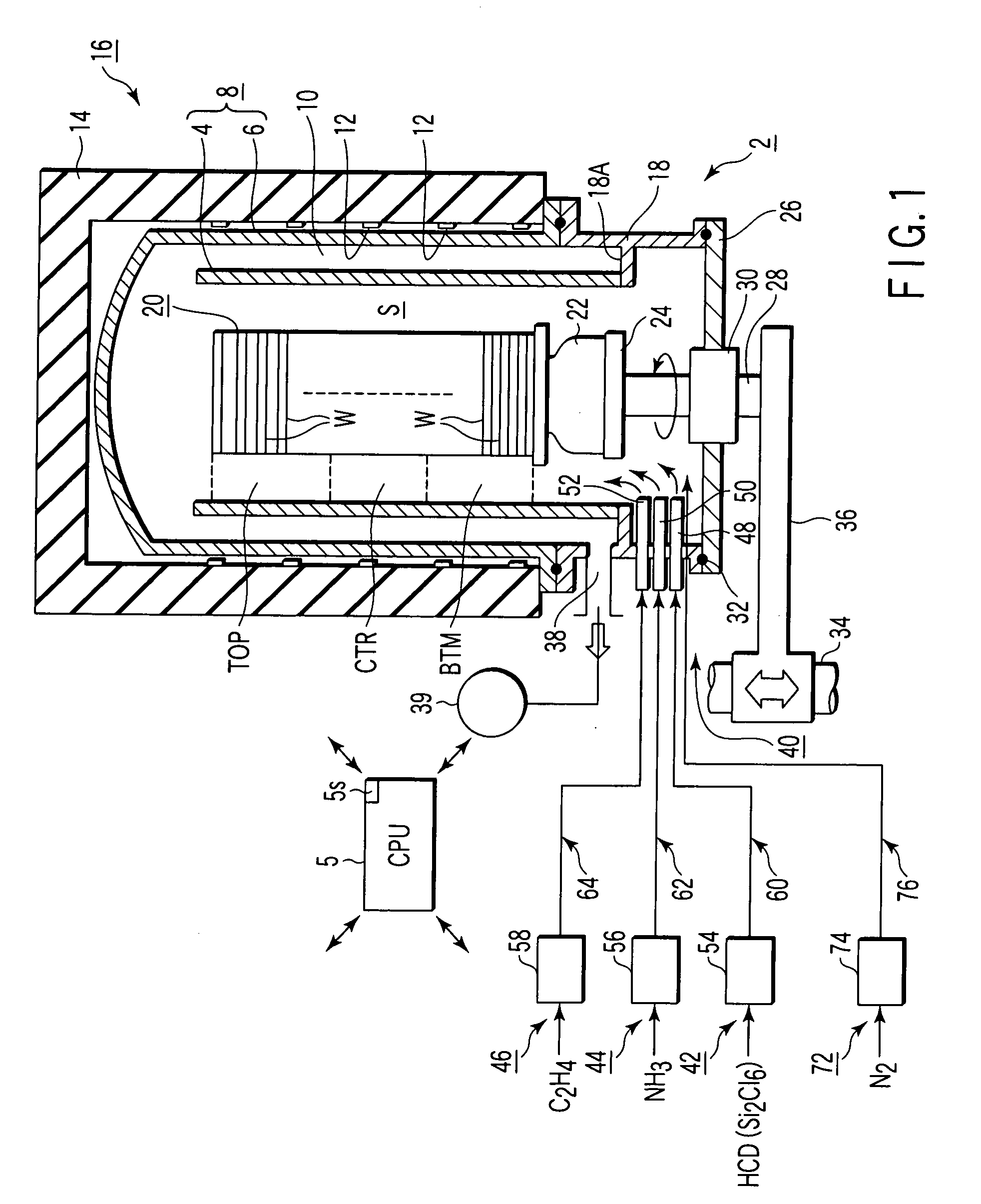
[0031]FIG. 1 is a sectional view showing a CVD apparatus according to an embodiment of the present invention. This CVD apparatus 2 is arranged to supply a first gas consisting essentially of a silane family gas (silicon source gas), a second gas consisting essentially of nitriding gas, and a third gas consisting essentially of a carbon hydride gas together, so as to form a silicon nitride film. For example, when hexachlorodisilane (HCD: Si2Cl6) and NH3 are used to deposit a silicon nitride film, a carbon hydride gas is supplied to make the film contain carbon components.

[0032] As shown in FIG. 1, this CVD apparatus 2 includes a process container 8 having a double tube structure, which is formed of an inner tube 4 and an outer tube 6. The inner tube 4 and outer tube 6 are formed of cylindrical quartz bodies, and disposed concentrically with each other with a predetermined gap 10 therebetween. The process container 8 is surrounded by a heating cover 16, which includes heating means 1...

first and second embodiments

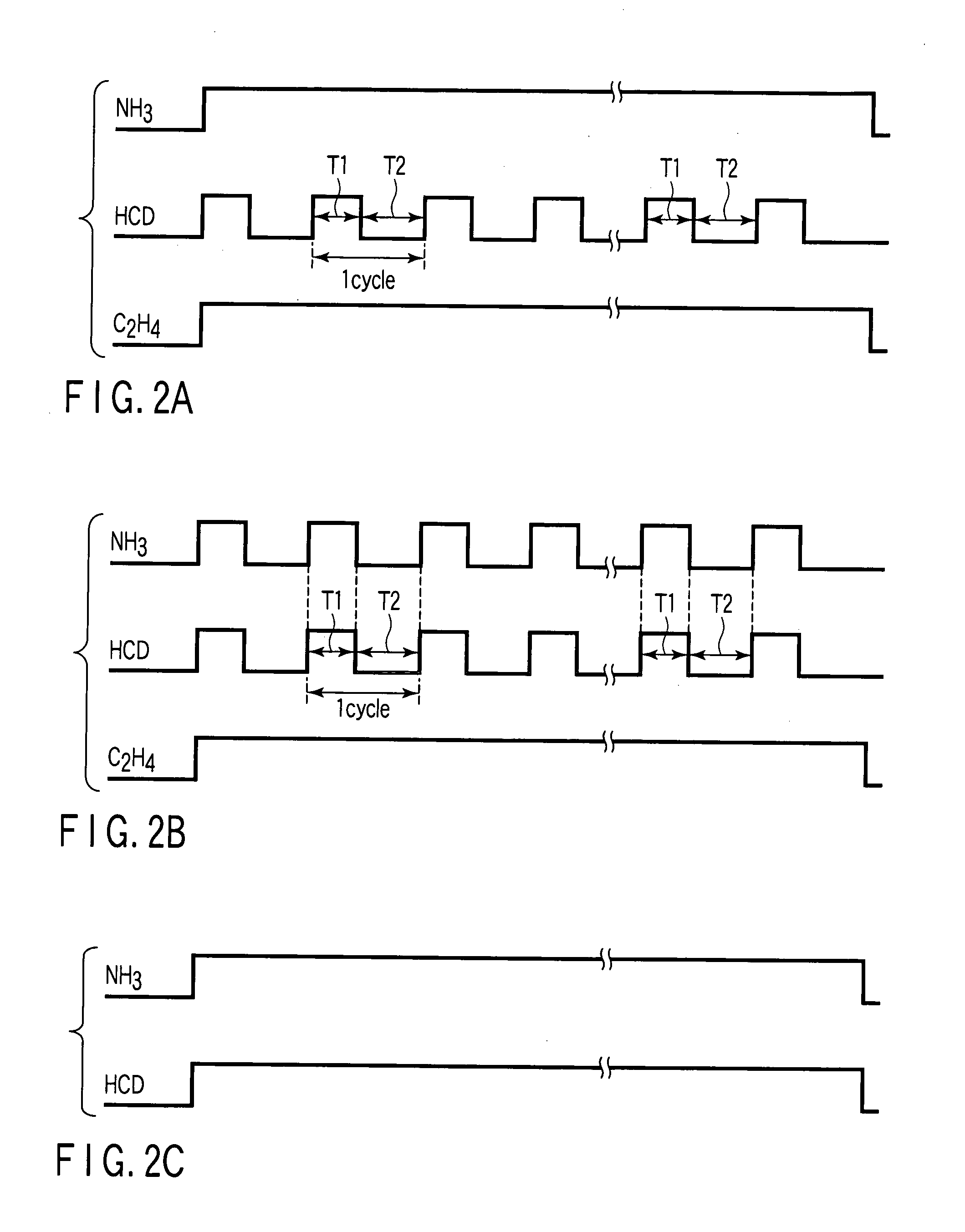
[0042]FIGS. 2A, 2B, and 2C are timing charts showing gas supply patterns according to first and second embodiments of the present invention and a prior art, respectively. As shown in FIGS. 2A and 2B, a HCD gas used as a silane family gas is not continuously supplied, but intermittently supplied, i.e., repeating start and stop of the supply. Specifically, according to the first embodiment, as shown in FIG. 2A, NH3 gas and C2H4 gas are continuously supplied. According to the second embodiment, as shown in FIG. 2B, C2H4 gas is continuously supplied, while NH3 gas is intermittently supplied in synchronism with the HCD gas. In the first and second embodiments, during one simultaneous supply period (deposition period) T1 of simultaneously supplying HCD gas and NH3 gas, a silicon nitride film containing carbon is deposited on the surface of wafers W. Further, during one recess period (reformation period) T2 of stopping supply of HCD gas, the silicon nitride film deposited immediately befor...

third embodiment

[0063]FIGS. 4A and 4B are timing charts showing gas supply patterns according to a third embodiment of the present invention and a modification thereof, respectively. According to the third embodiment shown in FIG. 4A, NH3 gas is continuously supplied, while C2H4 gas used as a carbon hydride gas is intermittently supplied, in synchronism with HCD gas being intermittently supplied. According to the modification of the third embodiment shown in FIG. 4B, NH3 gas is continuously supplied, while C2H4 gas used as a carbon hydride gas is intermittently supplied, in a cycle reverse to HCD gas being intermittently supplied. Specifically, as shown in FIG. 4B, supply of C2H4 gas is performed in the reformation period T2, and is stopped in the deposition period T1.

[0064]

[0065] In the first to third embodiments, the carbon hydride gas is exemplified by C2H4 (ethylene). In this respect, the carbon hydride gas may be one or more of gases selected from the group consisting of acetylene, ethylene, ...


PUM

PropertyMeasurementUnit
pressureaaaaaaaaaa
temperatureaaaaaaaaaa
heightaaaaaaaaaa

Abstract

A CVD method for forming a silicon nitride film includes exhausting a process chamber (8) that accommodates a target substrate (W), and supplying a silane family gas (HCD) and ammonia gas (NH3) into the process chamber, thereby forming a silicon nitride film on the target substrate by CVD. Said forming a silicon nitride film on the target substrate alternately includes a first period of performing supply of the silane family gas (HCD) into the process chamber (8), and a second period of stopping supply of the silane family gas.

Description

TECHNICAL FIELD [0001] The present invention relates to a CVD method and apparatus for forming a silicon nitride film on a target substrate, used in a semiconductor process. BACKGROUND ART [0002] Semiconductor devices include insulating films made of a material, such as SiO2, PSG (Phospho Silicate Glass), P—SiO (formed by plasma CVD), P—SiN (formed by plasma CVD), SOG (Spin On Glass), Si3N4 (silicon nitride), etc. Particularly, silicon nitride films are widely used, because they have better insulation properties as compared to silicon oxide films, and they can sufficiently server as etching stopper films. [0003] Some methods are known of forming a silicon nitride film on the surface of a semiconductor wafer by thermal CVD (Chemical Vapor Deposition). In such thermal CVD, a silane family gas, such as monosilane (SiH4), dichlorosilane (DCS: SiH2Cl2), hexachlorodisilane (HCD: Si2Cl6), or bistertialbutylaminosilane (BTBAS: SiH2(NH(C4H9)2), is used as a silicon source gas. For example, a...

Claims


Application Information

Patent Timeline
Patent Type & Authority Applications(United States)
IPC IPC(8): H01L21/31C23C16/34C23C16/44C23C16/455H01L21/318
CPCC23C16/345H01L21/3185C23C16/45523H01L21/02271H01L21/02211H01L21/0217H01L21/02115H01L21/324
Inventor KATO, HITOSHIFUKUSHIMA, KOHEIYONEZAWA, MASATOHIRAGA, JUNYA
Owner TOKYO ELECTRON LTD
Why Eureka
Try Eureka