Method of working nitride semiconductor crystal

a technology of nitride and semiconductor crystals, which is applied in the direction of grinding drives, manufacturing tools, grinding machine components, etc., can solve the problems of cracks or fractures, crack generation and waviness on the surface, and the difficulty of cutting such a nitride crystal, etc., to achieve simple and efficient manner and reduce costs.

Inactive Publication Date: 2006-12-28
SUMITOMO ELECTRIC IND LTD
View PDF10 Cites 11 Cited by
  • Summary
  • Abstract
  • Description
  • Claims
  • Application Information

AI Technical Summary

Benefits of technology

[0008] In view of the situation of the conventional art as described above, an object of the present invention is to provide a technique capable of working a nitride semiconductor crystal in a simple and efficient manner at lower costs.
[0010] The nitride semiconductor crystal can be cut using a wire electrode as the tool electrode. Preferably, the wire electrode is made of tungsten or molybdenum. In such a manner, a nitride semiconductor crystal substrate can be obtained by cutting an ingot of the nitride semiconductor crystal. Further, after cutting the nitride semiconductor crystal, a cut-surface of the crystal can be smoothed by sweeping the cut-surface again with the wire electrode. On the other hand, the nitride semiconductor crystal substrate obtained by the cutting may further be etched. In addition, the nitride semiconductor crystal substrate obtained by the cutting may further be polished.
[0012] With the cutting method according to the present invention, the nitride semiconductor crystal ingot can be cut so as to separate a peripheral portion thereof having low crystalline quality from a good crystal portion inside the ingot. More specifically, a through-hole is formed in the nitride semiconductor ingot and then the wire electrode is passed through the through-hole to make the through-hole a starting point for cutting in order to take out a good crystal inside the ingot without working the peripheral portion having low crystalline quality. With the working method according to the present invention, an edge at an end of a surface of the nitride semiconductor crystal can also be removed by inclining a longitudinal direction of the wire electrode at an angle in a range of 0-60° from a direction perpendicular to the surface of the nitride semiconductor crystal.

Problems solved by technology

However, since the nitride semiconductor crystal of GaN or the like among the compound semiconductors has high hardness and low toughness, it is difficult to cut such a nitride crystal by the same apparatus and method as those used for a Si crystal or a GaAs crystal, and there often arise problems such as crack generation and waviness on a surface formed by cutting (hereinafter referred to as a cut-surface).
Specifically, since the GaN crystal has low toughness, it is liable to cause cracks or fracture.
Further, since the GaN crystal has high hardness and is composed of two elements, distortion due to cutting easily occurs depending on distribution of hardness in the crystal.
In order to cut a GaN ingot with a good yield rate, therefore, it is necessary to reduce cutting load, which may cause reduction in throughput.
Although this peripheral region should be removed, grinding the periphery of the nitride semiconductor ingot is liable to cause cracks.
When the ingot is long, it is also difficult to work the long ingot with a core drill, resulting in severe wear of the tool.
Further, since such working needs abrasive grains and a grinding wheel, it requires higher costs.
Specifically, residual stress is concentrated in the polycrystalline portion in the peripheral region of the GaN ingot, and thus if balance of the stress is lost during the working, cracks are spontaneously generated due to poor strength of the crystal.
Furthermore, when the core drill is used to work the long ingot, it is difficult for a working fluid to permeate through a position to be worked, whereby making it difficult to provide satisfactory working.

Method used


Image

  • Method of working nitride semiconductor crystal
  • Method of working nitride semiconductor crystal
  • Method of working nitride semiconductor crystal

Examples


first example

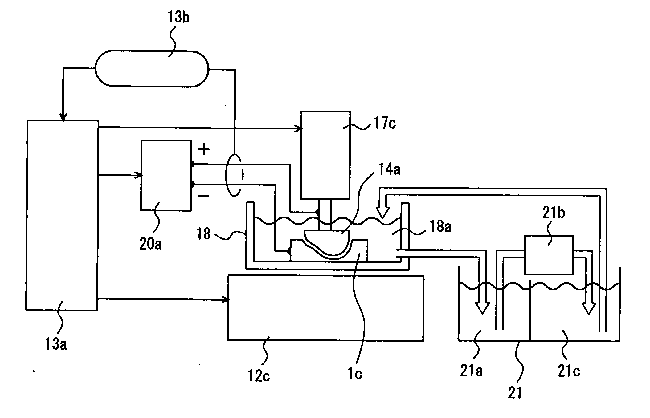
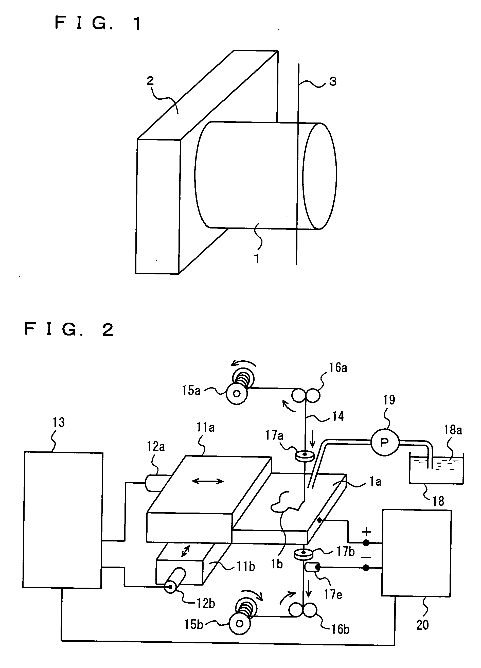
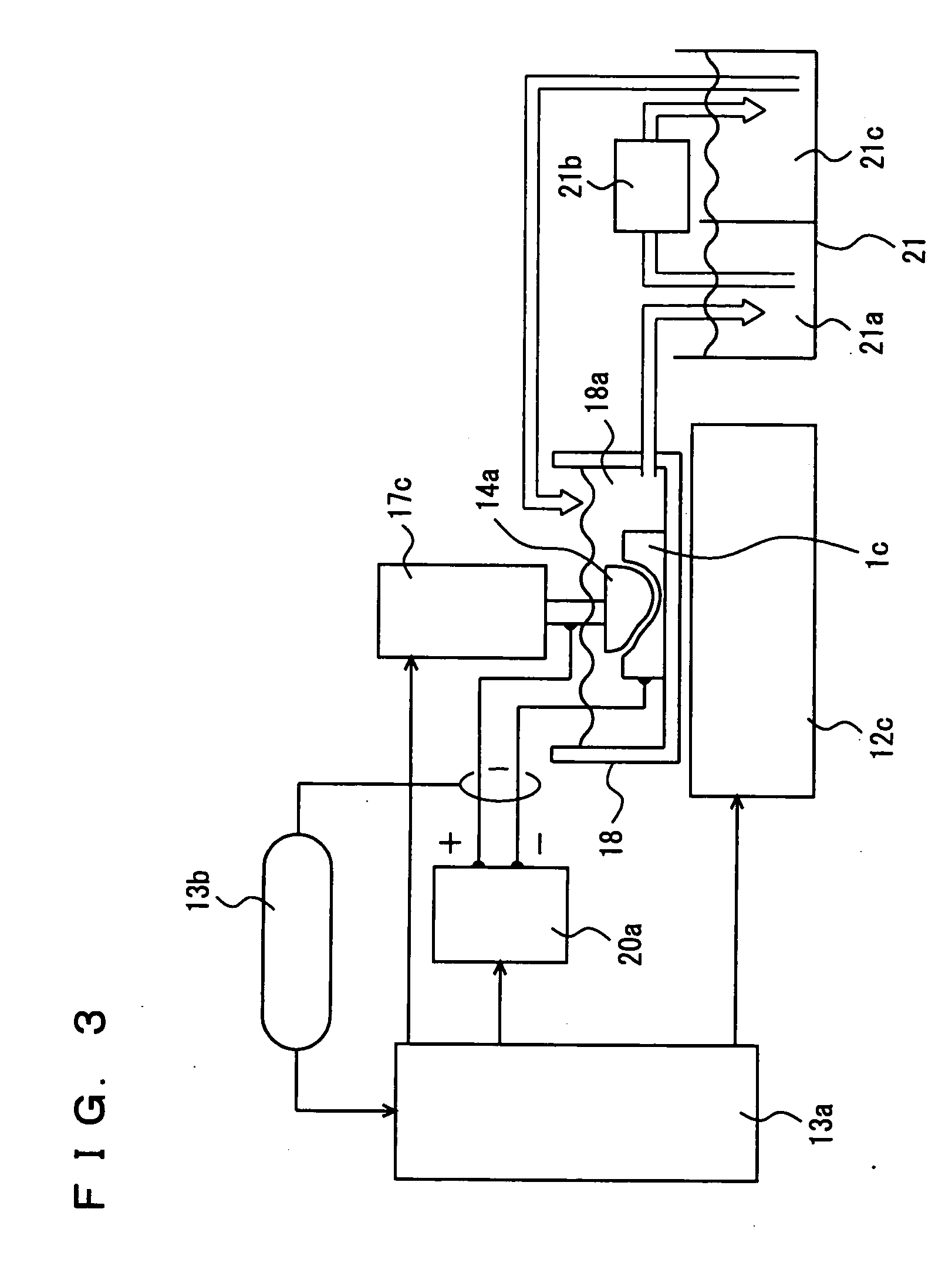
[0043] In a first example of the present invention, electrical discharge cutting was performed on a gallium nitride crystal having a diameter of 50 mm and a thickness of 30 mm grown by HVPE. This crystal contained oxygen as a dopant, and it had a carrier concentration of 4×1018 cm−3 and an electrical resistance of 1×10⁻² Ωcm. As shown in FIG. 1, crystal 1 was fixed to metal holder 2 with a conductive adhesive, and metal holder 2 was clamped to an electrical discharge machining apparatus. Wire electrode 3 of tungsten having a diameter of 0.1 mm was used (TWS-100 manufactured by Sumiden Fine Conductors). Cutting was performed on the crystal immersed in insulating water adjusted to have an electrical resistance of 70000 Ω. The wire was fed at a speed of 12 m / min, a working current was set at a value of 7, and a working voltage was set at 60 V. It took five hours to complete cutting under a constant electrical discharge condition with feeding-back of the voltage.

[0044] A substrate cut ...

second example

[0046] In a second example of the present invention, cutting was performed under similar conditions as those in the first example, except that a molybdenum wire having a diameter of 0.1 mm (TM-100 manufactured by Sumiden Fine Conductors) was used as the wire electrode. It also took five hours to complete cutting in the second example.

[0047] A substrate cut out had a thickness of 500 μm, and the cutting-loss as the width of the cutting groove was 150 μm. In addition, the substrate cut out had a warp of 15 μm. Further, the cut-surface of the substrate had a surface roughness Ra of 480 nm and a surface roughness Ry of 5200 nm.

third example

[0048] A third example of the present invention was different from the first example only in that a brass wire having a diameter of 0.15 mm (SS-15HN manufactured by Sumiden Fine Conductors) was used as the wire electrode and that cutting was performed with a working current set at a value of 11 and a working voltage set at 60 V. In the third example, it took two hours to complete cutting, enabling cutting in a short period of time. On the other hand, since the wire electrode used in the third example had a larger diameter than that in the first example, the cutting-loss increased to 190 μm.


PUM

PropertyMeasurementUnit
angleaaaaaaaaaa
flatnessaaaaaaaaaa
flatnessaaaaaaaaaa

Abstract

In a method of working a crystal, when a nitride semiconductor crystal is worked, voltage is applied between the nitride semiconductor crystal and a tool electrode to cause electrical discharge, so that the crystal is partially removed and worked by local heat generated by the electrical discharge.

Description

BACKGROUND OF THE INVENTION [0001] 1. Field of the Invention [0002] The present invention relates to a method of working a semiconductor crystal, and more particularly to a method of working a nitride semiconductor crystal. [0003] 2. Description of the Background Art [0004] Generally, a cutting tool such as an inner diameter blade or a wire saw is used to cut out a substrate from a semiconductor crystal ingot of silicon or the like. A compound semiconductor crystal ingot of GaAs, InP or the like is also cut with a multi-wire saw, as described in Japanese Patent Laying-Open No. 09-017755, for example. [0005] Among compound semiconductors, a nitride semiconductor crystal of GaN or the like has a wide energy band gap, and thus it is in increasing demand as a semiconductor suitable for an LED (light emitting diode) or an LD (laser diode) capable of emitting short-wavelength light. Accordingly, it is desired to work a grown crystal ingot of a nitride semiconductor in a simple and efficie...

Claims


Application Information

Patent Timeline
Patent Type & Authority Applications(United States)
IPC IPC(8): H01L21/00B23H9/00B24B47/22H01L21/304
CPCB23H7/02H01L21/3043B23H9/00
Inventor ISHIBASHI, KEIJIHACHIGO, AKIHIRONISHIURA, TAKAYUKI
Owner SUMITOMO ELECTRIC IND LTD
Why Eureka
Try Eureka