

Silver barrier layers to minimize whisker growth in tin electrodeposits
a technology of silver barrier layer and tin electrode, which is applied in the direction of semiconductor/solid-state device testing/measurement, semiconductor/solid-state device details, instruments, etc., can solve the problems of excessive stress formation in the tin deposit, undesirable presence of whiskers, and whiskers that may create shorts or introduce failures into electronic circuits, etc., to achieve greater load and stringent test
- Summary
- Abstract
- Description
- Claims
- Application Information
AI Technical Summary
Benefits of technology
Problems solved by technology
Method used
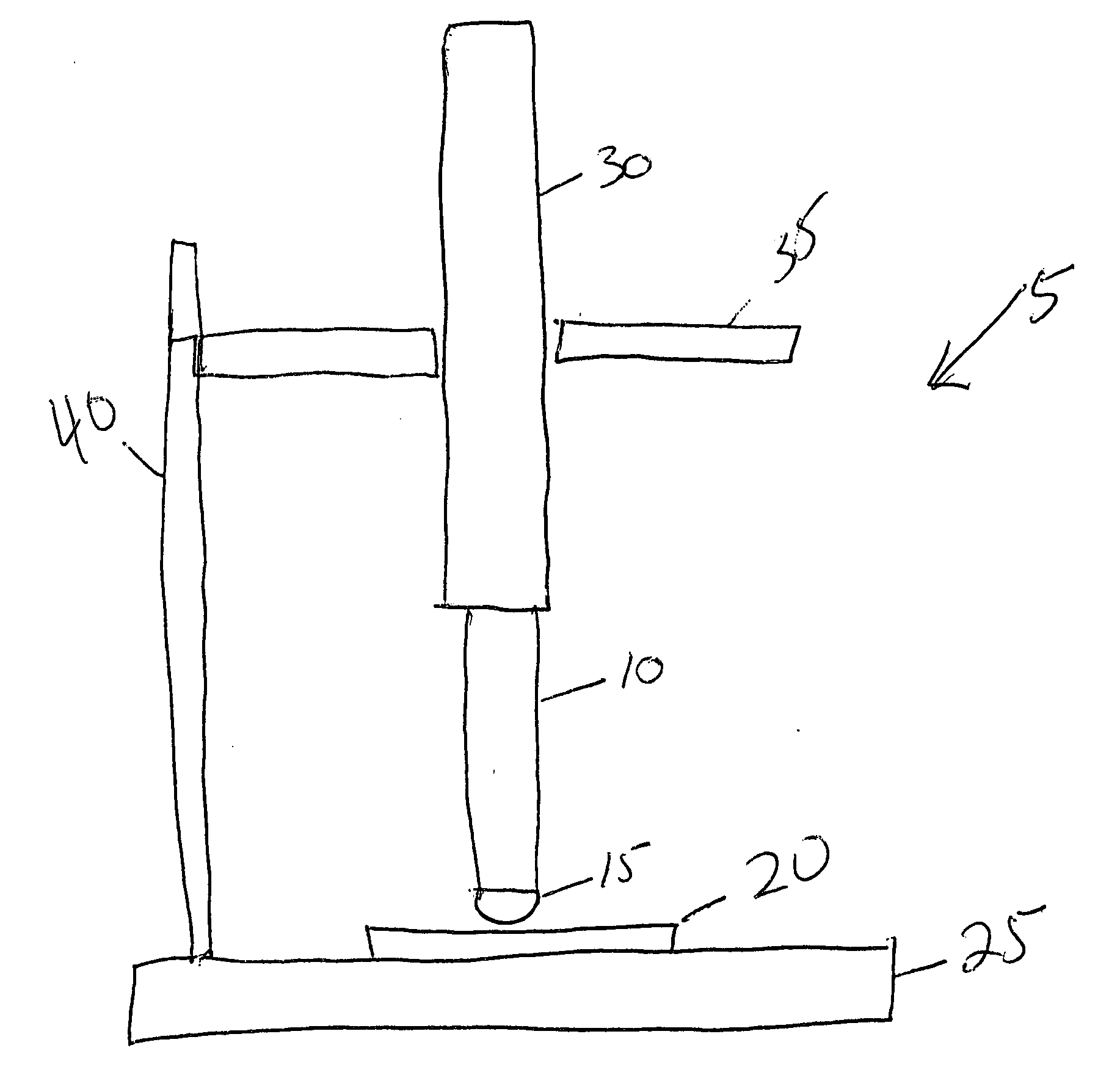
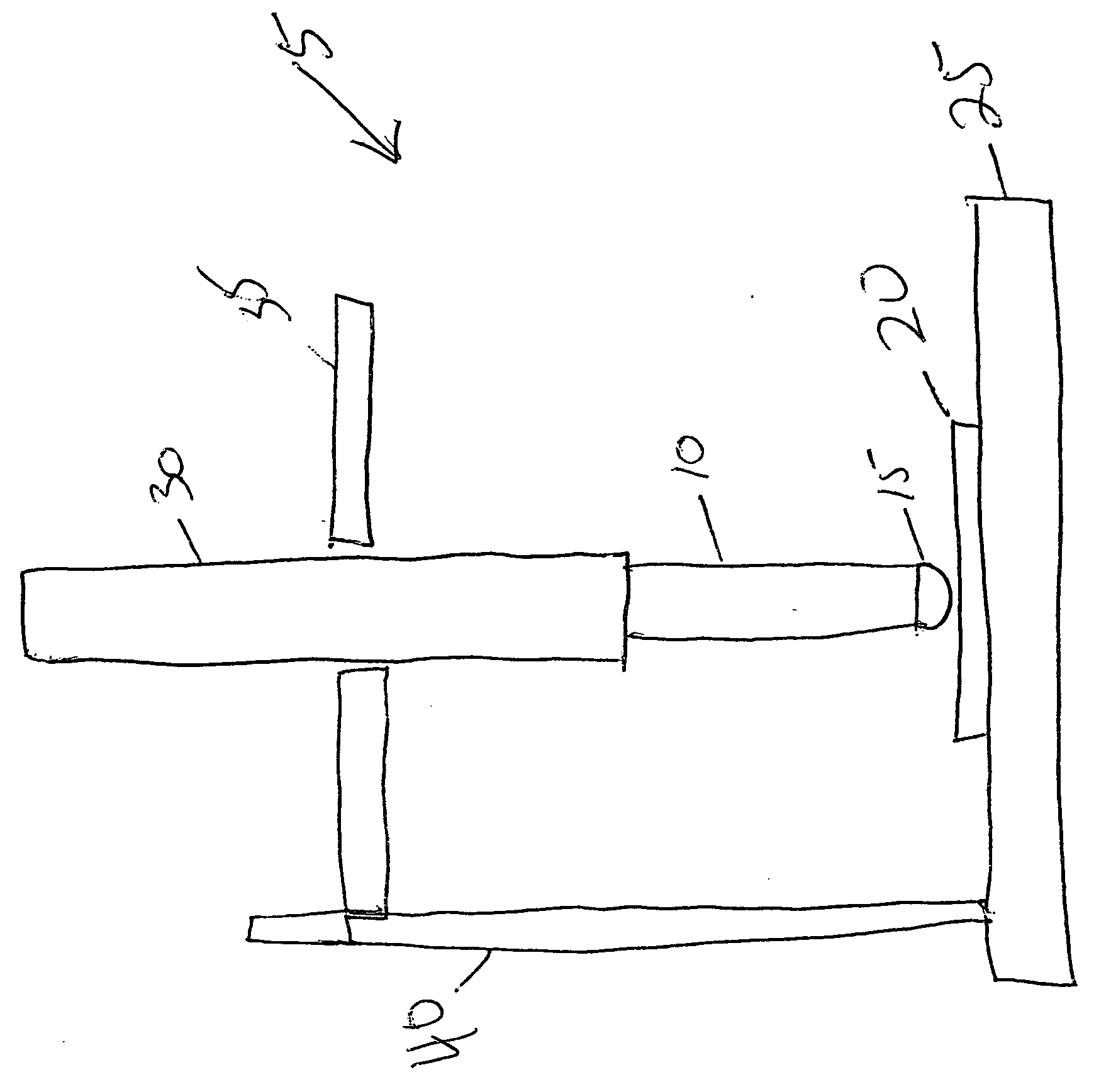
Image

Examples
examples
[0041] The following examples illustrate the most preferred embodiments of the invention.
Example (1)
[0042] Tin was electroplated from an MSA electrolyte onto a Cu alloy substrate (Cu99.85%, Sn0.15%) at a current density of 100 A / ft2 for a period of time sufficient to obtain an average of 10 μm tin deposit thickness. The deposit was subjected to the three whisker test conditions specified by JEDEC STANDARD JESD22A121 “Measuring Whisker Growth on Tin and Tin Alloy Surface Finishes”, specifically: (i) thermal cycling −40° C. to +85° C. for 1000 cycles; (ii) ambient storage (30° C., 60% RH) for min. 3000 hrs; and (iii) high temperature / humidity storage (60° C. / 90% RH) for min. 3000 hrs. Upon completion of the whisker test method, the maximum whisker length was measured and determined to be 78 μm.
Example (2)
[0043] Nickel barrier layer was plated from a commercial nickel sulfamate electrolyte (Techni Nickel FFP from Technic Inc.) onto a Cu alloy substrate (Cu99.85%, Sn0.15%) at a curr...
example
(11)
[0052] Silver barrier layer was plated from a commercial silver cyanide electrolyte (Techni Silver EHS-3 from Technic Inc.) onto a Cu alloy substrate (Cu99.85%, Sn0.15%) at a current density of 50 A / ft2 for a period of time sufficient to obtain an average of 0.15 μm silver deposit thickness, then tin was electroplated on the silver barrier layer from an MSA electrolyte at a current density of 100 A / ft2 for a period of time sufficient to obtain an average of 10 μm tin deposit thickness. The electroplated part was then subjected to reflow in a convection oven at 280 deg C for 3 min. The reflowed deposit was then subjected to the mechanical load whisker test described previously for 48 hrs. Upon completion of the whisker test method, the maximum whisker length was measured and determined to be <2 μm.
PUM
| Property | Measurement | Unit |
|---|---|---|
| length | aaaaa | aaaaa |
| length | aaaaa | aaaaa |
| thickness | aaaaa | aaaaa |
Abstract
Description
Claims
Application Information