Interlayer insulating layer for printed wiring board, printed wiring board and method for manufacturing same

a technology of interlayer insulating layer and printed wiring board, which is applied in the directions of printed circuit aspects, conductive pattern formation, transportation and packaging, etc., can solve the problems of reducing the thermal expansion coefficient of the interlayer dielectric layer, reducing connection reliability, and incurring such low connection reliability, so as to reduce the expansibility or contractility, effectively inhibit the expansion or contraction of the resin, and reduce the coefficient of thermal expansion

Inactive Publication Date: 2007-01-18
IBIDEN CO LTD
View PDF7 Cites 59 Cited by
  • Summary
  • Abstract
  • Description
  • Claims
  • Application Information

AI Technical Summary

Benefits of technology

[0067] In the interlayer dielectric layer according to the present invention for printed wiring boards, the particles dispersed in the curable resin are flaky in shape. So, different from any spherical particles, the flaky particles are dispersed at all angles in relation to the substrate surface. As the dielectric layer expands or contracts, the flaky particles will also move at the same time. However, since the particles dispersed at all angles in relation to the substrate surface collide with each other, a friction will occur between the particles and also between the particles and resin, and the expansion or contraction of the interlayer dielectric layer will thus be constricted (which will be referred to as “three-dimensional constraint effect” hereunder).
[0068] Also, since each of the flaky particles has a larger surface area than the spherical particle and the intermolecular force between the flaky particles and resin is larger than that between the spherical particles and resin, so the mutual adhesion between the flaky particles and resin is larger than that between the spherical particles and resin. Thus, the flaky particles are smaller in expansibility or contractility than the resin, and so they effectively inhibit the resin from expanding or contracting (which will be referred to as “inhibit effect” hereunder).
[0069] In the interlayer dielectric layer according to the present invention for printed wiring boards, the flaky particles having a relatively small coefficient of thermal expansion are dispersed in the resin having a relatively large coefficient of thermal expansion and will have a synergy of the three-dimensional constraint effect and inhibit effect. So, even a smaller amount of the flaky particles dispersed in the resin than that of spherical particles, if used, will lead to a smaller coefficient of thermal expansion of the resultant dielectric layer. Therefore, a printed wiring board including the interlayer dielectric layer according to the present invention and a circuit board including the interlayer dielectric layer and on which semiconductor devices are to be mounted will have an improved cooling/heating cycle resistance.
[0070] Among others, the above-mentioned synergy of the three-dimensional constraint effect and inhibit effect will result in a coefficient of thermal expansion α2 in a temperature domain in which the resin is at a higher temperature than the glass transition temperature (will be referred to simply as “Tg” hereunder). Normally, the coefficient of thermal expansion α2 will be three times larger at a temperature higher than Tg than that α1 at a temperature lower than Tg. However, the synergy of the three-dimensional co

Problems solved by technology

Since the air-containing dielectric layer of the IC chip is fragile, it is necessary to further reduce the coefficient of thermal expansion of the interlayer dielectric layer.
However, if the content of the particles is excessive, the particles will remain in the viahole, leading to a lower connection reliability.
Especially, viaholes of less than 70 μm in opening diameter will incur such lower connection reliability.
Therefore, it is difficult to form a fine pattern of less than 15 μm/15 μm in L/S (line width/interline space), and the irregularity of the interlayer dielectric layer surface makes it difficult to form an interlayer dielectric layer having a uniform thickness.
Thus, it is also difficult to control the impedance in transmitting a signal of 3 GHz or higher in frequency.
The above-mentioned conventional pattern-forming method is not advantageous in that a pattern having a one-to-one relation with the pattern of the photo mask cannot be formed because of the influence of the light diffraction and miniaturization of the pattern is limited because the resist will be made to fly in all directions under a pressure applied during spray development.
That is, no multilayering is possible.
However, it is difficult to heat only the second interlayer dielectric layer.
The wiring pattern formed in the first interlayer dielectric layer will move, resulting in misalignment with an upper layer, short-circuiting between adjacent patterns and crushing of the interlayer dielectric layer under the pressure.
Secondly, it is difficult to maintain, after the mold is removed, the shape of the wiring pattern-forming groove transcribed from the mold to the interlayer dielectric layer and shape of the viahole-formin

Method used


Image

  • Interlayer insulating layer for printed wiring board, printed wiring board and method for manufacturing same
  • Interlayer insulating layer for printed wiring board, printed wiring board and method for manufacturing same
  • Interlayer insulating layer for printed wiring board, printed wiring board and method for manufacturing same

Examples


embodiment 1

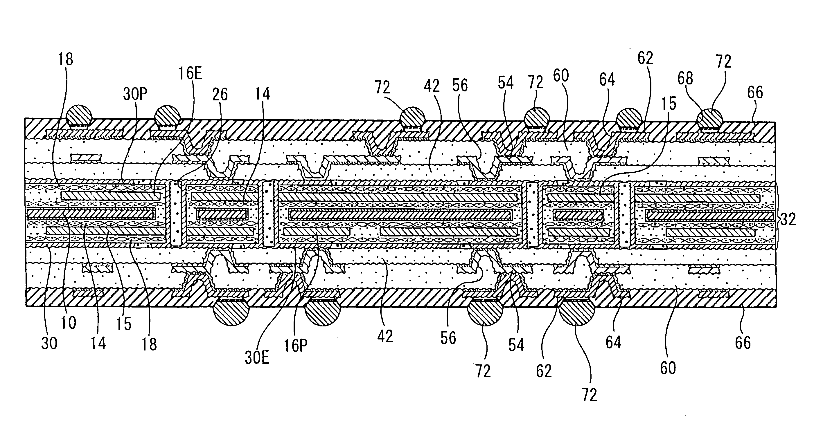
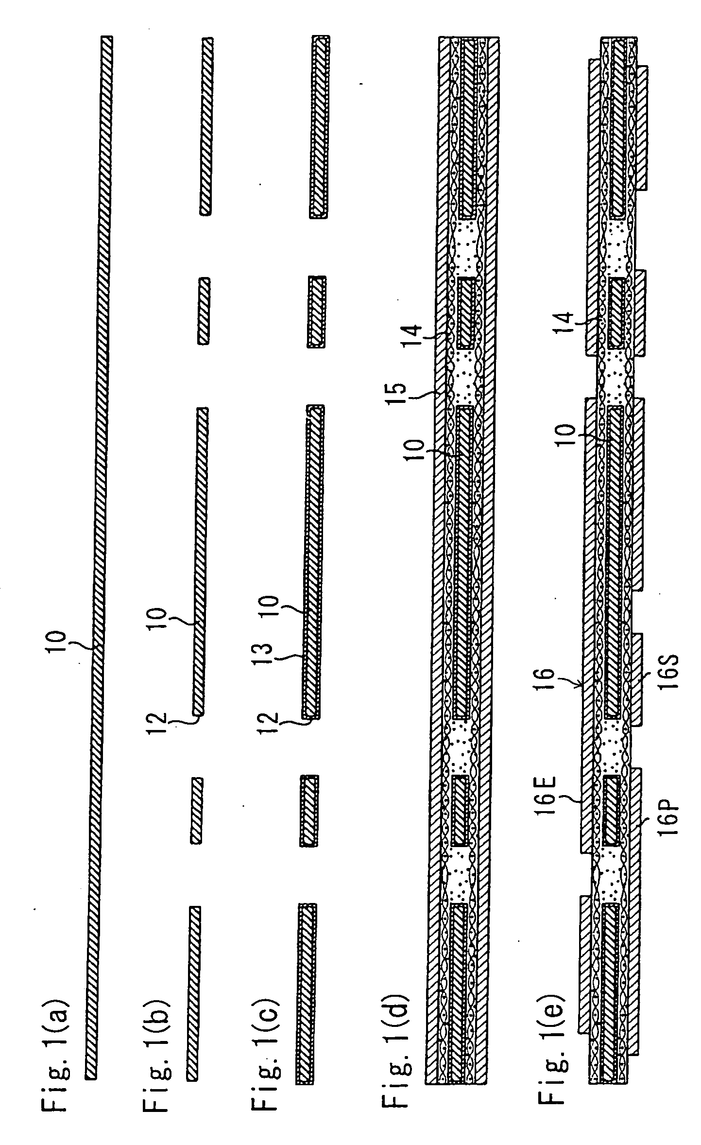
[0204] (A) Preparing a Kneaded Mixture Containing Flaky Particles

[0205] Fifteen grams of flaky particles (“ESPEN C” by the HOJUN; about 500 in aspect ratio when the particles are dispersed; about 0.5 μm in crystal size) was added to a mixed solvent containing 20 g of methyl ethyl ketone (will be referred to as “MEK” hereunder) and 80 g of xylene, and this mixture was kneaded using three rollers to prepare a kneaded mixture containing the flaky particles.

[0206] (B) Preparing a Solution Containing Epoxy Resin

[0207] Eighty five grams of solid epoxy resin (“EPICOAT 1007” by the Japan Epoxy Resin) was added to the mixed solvent containing 6.8 g of MEK and 27.2 g of xylene, and the resin and mixture were mixed together to prepare a solution containing the epoxy resin.

[0208] (C) Preparing a Resin Film for the Interlayer Dielectric Layer

[0209] The kneaded mixture containing the flaky particles, prepared in step (A) above, the solution containing the epoxy resin, prepared in step (B), d...

embodiment 2

[0295] A multilayer printed wiring board was produced similarly to the embodiment 1 except that the flaky particle used was “NANOFIL” (by the TOPY INDUSTRY; 100 to 500 in aspect ratio after the particles are dispersed; 0.1 to 0.5 μm in size; 0.001 μm in minimum particle thickness).

embodiment 3

[0296] A multilayer printed wiring board was produced similarly to the embodiment 1 except that the kneaded mixture containing flaky particles and solution containing epoxy resin were prepared as in processes (A) and (B) below:

[0297] (A) Preparing a Kneaded Mixture Containing Flaky Particles

[0298] Fifteen grams of flaky particles (“ESPEN C” by the HOJUN; about 500 in aspect ratio when the particles are dispersed; about 0.5 μm in crystal size) was added to a mixed solvent containing 33 g of MEK and 67 g of xylene, and this mixture was kneaded using three rollers to prepare a kneaded mixture containing the flaky particles.

[0299] (B) Preparing a Solution Containing Epoxy Resin

[0300] Eighty five grams of solid epoxy resin (“EPICOAT 1007” by the Japan Epoxy Resins) was added to the mixed solvent containing 11 g of MEK and 23 g of xylene, and the resin and mixture were mixed together to prepare a solution containing the epoxy resin.


PUM


Abstract

A printed wiring board is provided which includes an interlayer dielectric layer formed on a substrate from a curable resin having flaky particles dispersed therein. The printed wiring board is excellent in cooling/heating cycle resistance and packaging reliability while maintaining a satisfactory heat resistance, electrical insulation, heat liberation, connection reliability and chemical stability. Also a method of producing a printed wiring board is proposed in which an imprint method using a mold having formed thereon convexities corresponding to wiring patterns and viaholes to be formed being buried in an interlayer dielectric layer is used to form the wiring patterns and viaholes by transcribing the concavities of the mold to the interlayer dielectric layer. The imprint method permits to form the wiring patterns and viaholes but assures an easy and accurate transcription without any optical transcription or complicated etching. Thus, a multilayer printed wiring board excellent in insulation reliability and interlayer connection and having fine wiring patterns formed therein can be mass-produced extremely easily and inexpensively.

Description

FIELD OF THE INVENTION [0001] The present invention relates to an interlayer dielectric layer formed by curing an interlayer dielectric material for a printed wiring board, a printed wiring board including the interlayer dielectric layer, and a method of producing the printed wiring board. BACKGROUND ART [0002] With the recent evolution of the electronics, there have been required printed circuit boards and wiring boards on which at least one LSI is to be mounted, formed to have a finer wiring pattern that assures a higher packaging density and reliability for a more compact design of electronic devices and higher speed of signal transmission. [0003] On this account, it has recently been proposed to form a conductor circuit on a wiring board by applying an interlayer dielectric material to the surface of a substrate to form an interlayer dielectric layer, roughing the surface of the interlayer dielectric layer and forming the circuit by the additive or semi-additive method. [0004] A...

Claims


Application Information

Patent Timeline
IPC IPC(8): H01L23/24H05K3/00H05K3/04H05K3/10H05K3/46
CPCH01L23/145Y10T428/25H01L23/49827H01L2924/3011H05K3/005H05K3/045H05K3/107H05K3/381H05K3/4602H05K3/465H05K3/4661H05K2201/0209H05K2201/0212H05K2201/0245H05K2201/09036H05K2203/0108H05K2203/1152H05K2203/1189H01L2224/16225H01L2924/15311H01L23/49822H01L2924/12044H01L2224/05573H01L2224/05568H01L2924/00014H01L2224/0554H01L2924/00H01L2224/05599H01L2224/0555H01L2224/0556H05K3/46
Inventor ASAI, MOTOONODA, KOUTAINAGAKI, YASUSHI
Owner IBIDEN CO LTD
Why Eureka
Try Eureka